Crystal particle granule solar battery and manufacturing method thereof
A technology of solar cells and crystals, applied in the field of solar cells, can solve problems such as current leakage and short circuit, and achieve the effects of low energy consumption, reduced manufacturing costs, and high material utilization
- Summary
- Abstract
- Description
- Claims
- Application Information
AI Technical Summary
Problems solved by technology
Method used
Image
Examples
Embodiment 1
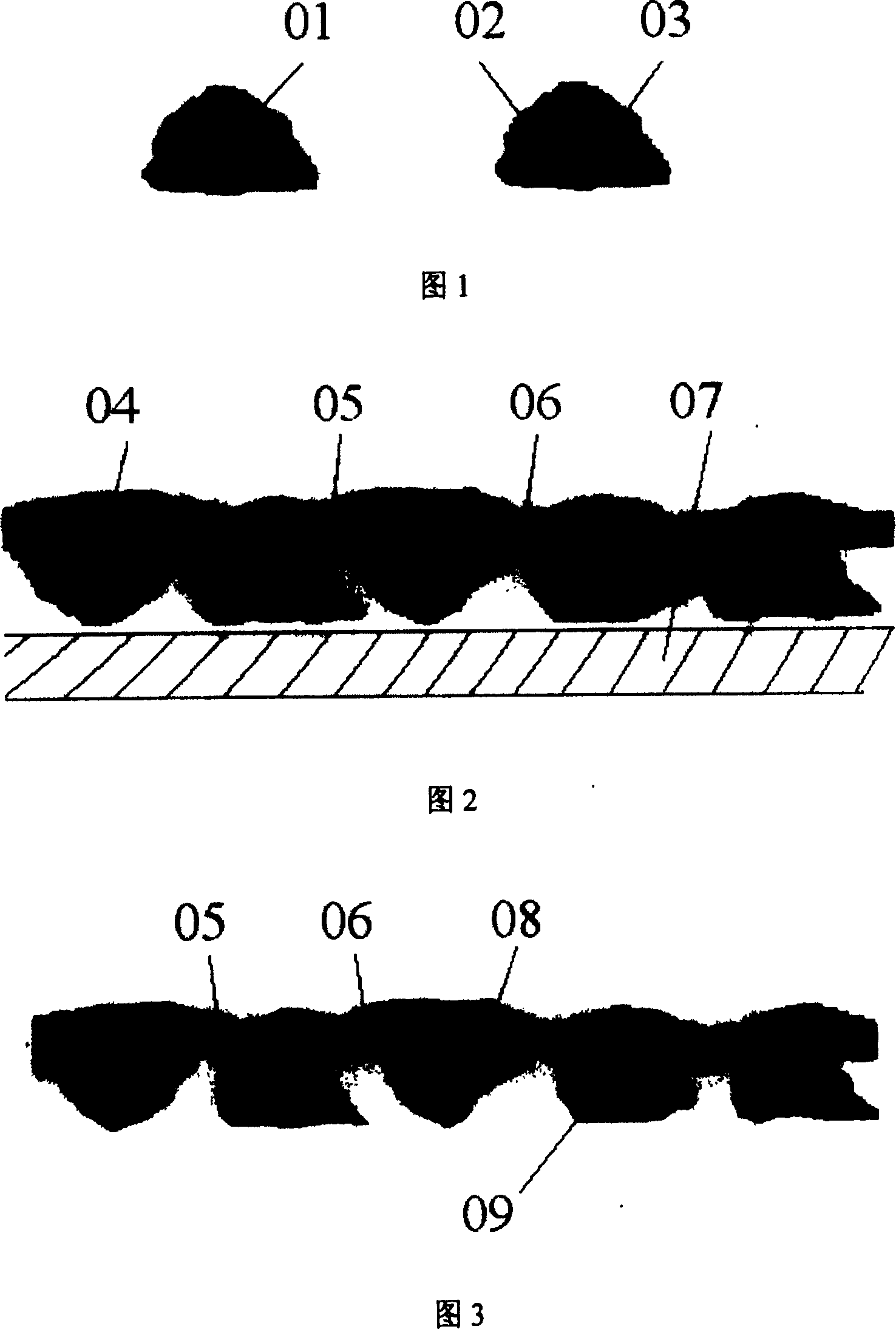
[0048] The solar-grade P-type polysilicon material with a resistivity of 5 ohm cm is crushed into silicon particles, and after screening, the particles with a size of 0.3 mm to 0.4 mm are selected. After the selected silicon particles are cleaned, phosphorus is diffused. The diffusion method used is the same as the method for preparing polycrystalline silicon or single crystal silicon solar cells. The outer surface is N and the inner is P-type wrapping structure. PN junction, as shown in Figure 1. The diffusion temperature is 900°C, nitrogen protection and a small amount of oxygen are introduced during the diffusion, so that a very thin oxide layer is formed on the outermost part of the particles.
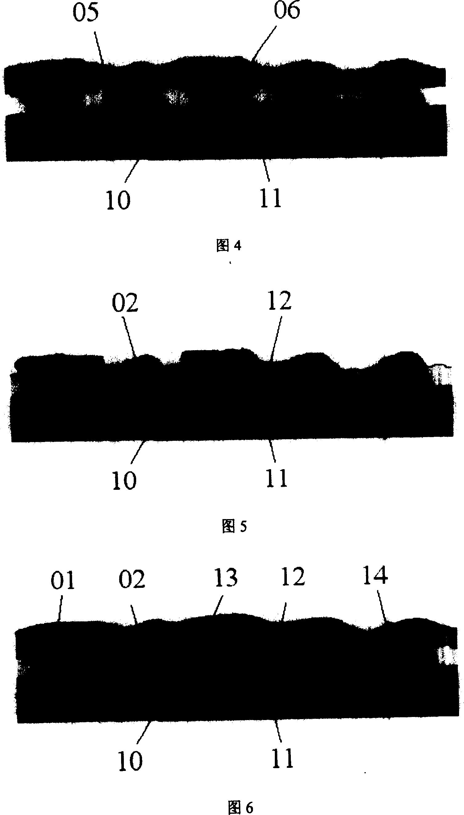
[0049] Spread the silicon particles with diffused PN junction densely on a plane, and apply appropriate vibration to make the particles densely arranged, and at the same time ensure that the particles are arranged in a single layer without stacked particles, as shown in Figure 2. A...
Embodiment 2
[0056] The solar-grade P-type polysilicon material with a resistivity of 5 ohm cm is crushed into silicon particles, and after screening, the particles with a size of 0.3 mm to 0.4 mm are selected. After the selected silicon particles are cleaned, phosphorus is diffused on the surface to form a wrapping structure with N on the outer surface and P-type inside, and a PN junction in the crystal grain, as shown in Figure 2. The diffusion temperature is 900°C, nitrogen protection and a small amount of oxygen are introduced during the diffusion, so that the outermost layer of the particles will have an insulating layer of oxide and / or silicon nitride.
[0057] Spread the silicon particles with diffused PN junction densely on a plane, and apply appropriate vibration to make the particles densely arranged, and at the same time ensure that the particles are arranged in a single layer without stacked particles, as shown in Figure 3. After such The area occupied by the treated silicon pa...
PUM
| Property | Measurement | Unit |
|---|---|---|
| thickness | aaaaa | aaaaa |
| thickness | aaaaa | aaaaa |
| size | aaaaa | aaaaa |
Abstract
Description
Claims
Application Information
 - R&D
- Intellectual Property
- Life Sciences
- Materials
- Tech Scout
- Unparalleled Data Quality
- Higher Quality Content
- 60% Fewer Hallucinations
Browse by: Latest US Patents, China's latest patents, Technical Efficacy Thesaurus, Application Domain, Technology Topic, Popular Technical Reports.
© 2025 PatSnap. All rights reserved.Legal|Privacy policy|Modern Slavery Act Transparency Statement|Sitemap|About US| Contact US: help@patsnap.com


