

Method for producing ceramic substrate
A manufacturing method and technology of ceramic substrates, which are applied in the direction of improving the metal adhesion of insulating substrates, manufacturing printed circuits, and manufacturing multilayer circuits, etc., and can solve problems such as the adhesive layer cannot be covered, the adhesion is insufficient, and peeling off
- Summary
- Abstract
- Description
- Claims
- Application Information
AI Technical Summary
Problems solved by technology
Method used
Image

Examples
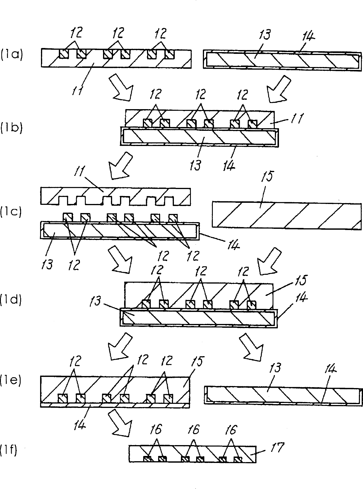
Embodiment 1
[0062] Example 1 will be described with reference to FIG. 1 . In the thick-film gravure copying, a heat-resistant film such as polyimide is used for the gravure.
[0063] This film is machined with grooves as a conductor pattern by a stimulated complex laser, thereby forming a gravure film. This relief film is peeled off so that it can be easily peeled off during gravure copying. Use a rigid scraper to fill the conductor pattern groove with conductor paste for the film groove. Conductor paste adopts silver-based paste that can be fired to 850°C to 900°C. The gravure film filled with the paste is dried in a dryer at 100°C to 150°C for 5 to 10 minutes. The conductor paste filled into the grooves reduces in volume due to evaporation of the solvent in the paste after drying. In order to make the concavity of the dry surface of the conductive paste on the unprocessed side of the gravure film less than 5 μm, the conductive paste should be repeatedly filled and dried.
[0064] T...
Embodiment 2
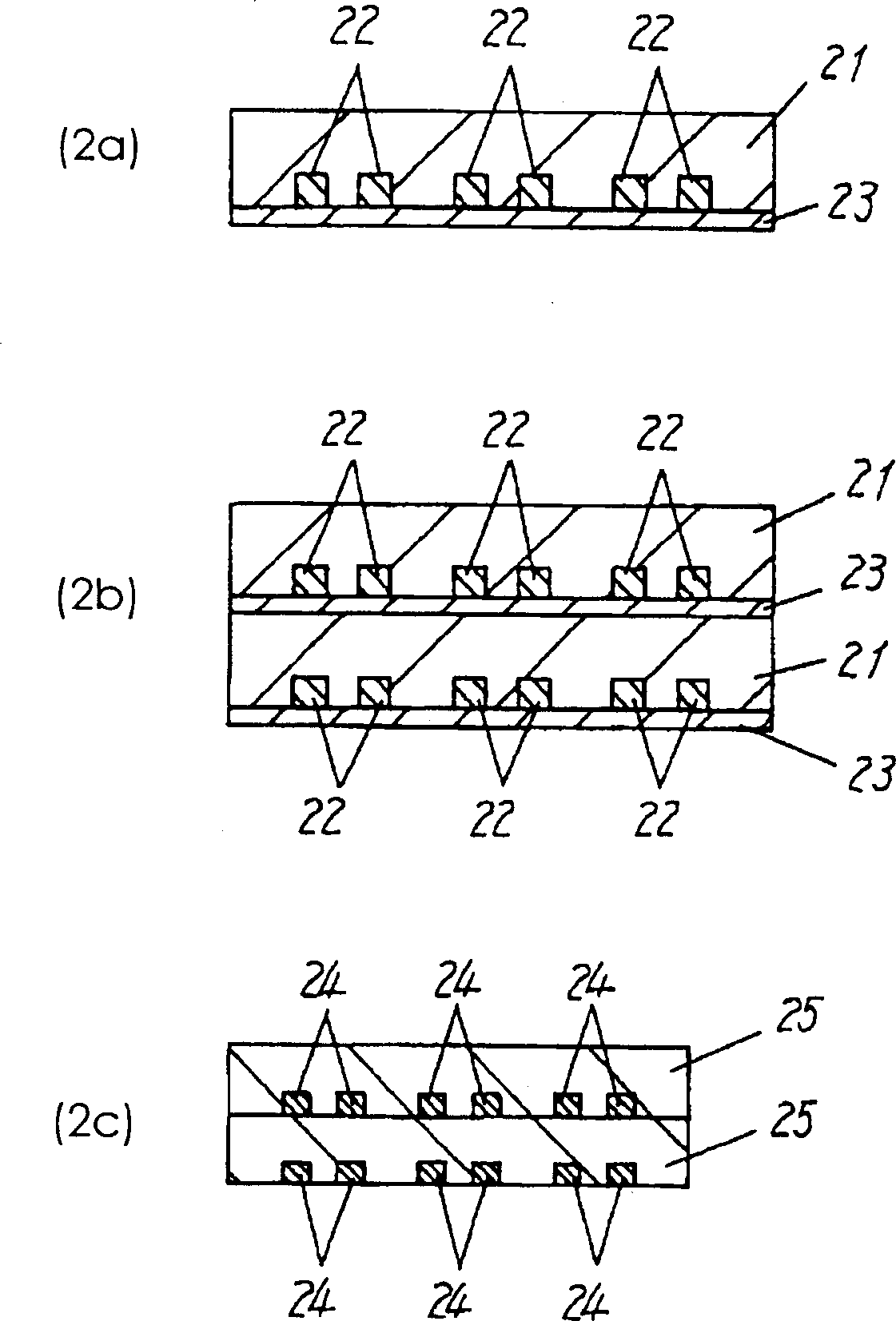
[0068] Embodiment 2 will be described based on FIG. 2 . Two or more unsintered ceramic green sheets obtained by re-transferring by the thick-film gravure replication method in Example 1 were stacked and integrated by hot pressing. The hot pressing temperature at this time needs to be higher than the softening temperature of the adhesive layer and lower than the critical temperature (about 100° C.) at which the GS does not thermally deform. The hot-pressing pressure is about 50-100kg / cm2, and the hot-pressing time is about 3-10 minutes, but it can be adjusted according to the laminated state so that the laminated part does not peel off.
[0069] Secondly, by debonding and sintering this GS, ceramic multilayer circuit boards with high-density conductor patterns can be manufactured.
Embodiment 3
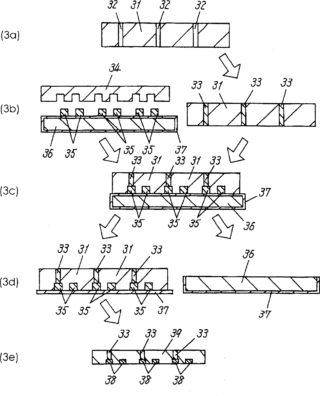
[0071] Embodiment 3 will be described based on FIG. 3 . Through-holes were formed in green ceramic green sheets (hereinafter abbreviated as GS) before re-replication by the thick-film gravure replication method in Example 1 using a punching device or the like. Fill the conductive paste on the through hole with a metal plate by screen printing, and dry it at a temperature (60-100°C) that does not deform the GS. Then, as in Example 1, the heat-resistant substrate temporarily filled with the conductor paste and the GS on which the via-hole conductors were formed were hot-pressed, and the conductor paste was transferred to the side of the GS on which the via-hole conductors were to be formed. Then, the heat-resistant substrate is peeled off, and GS with conductive patterns and through-hole conductors formed by the gravure film can be manufactured. In this way, a ceramic circuit substrate having a high-density conductor pattern connected by interlayer via holes can be manufactured...
PUM
| Property | Measurement | Unit |
|---|---|---|
| thickness | aaaaa | aaaaa |
Abstract
Description
Claims
Application Information