Flash memory cell and its preparing process

A storage unit and flash technology, applied in semiconductor/solid-state device manufacturing, electrical components, electric solid-state devices, etc., can solve problems such as poor reliability of high-power consumption storage units

Inactive Publication Date: 2002-12-25
TSINGHUA UNIV
View PDF0 Cites 20 Cited by
  • Summary
  • Abstract
  • Description
  • Claims
  • Application Information

AI Technical Summary

Problems solved by technology

It is a kind of flash memory unit that adopts source enhanced strip band tunneling hot electron injection for writing operation, which can

Method used


Image

  • Flash memory cell and its preparing process
  • Flash memory cell and its preparing process
  • Flash memory cell and its preparing process

Examples


Embodiment Construction

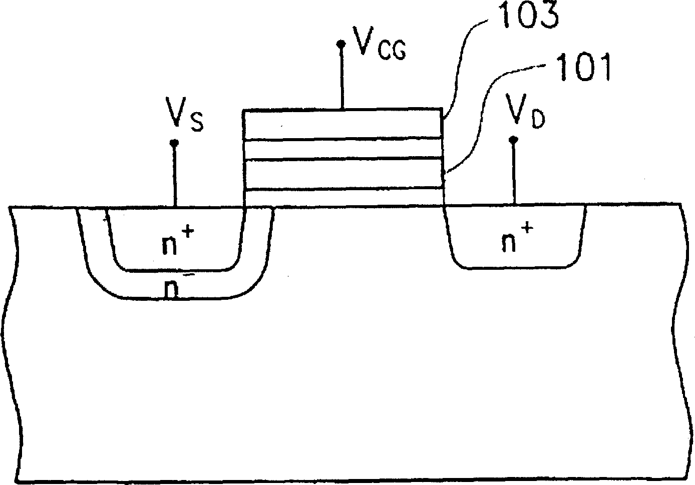
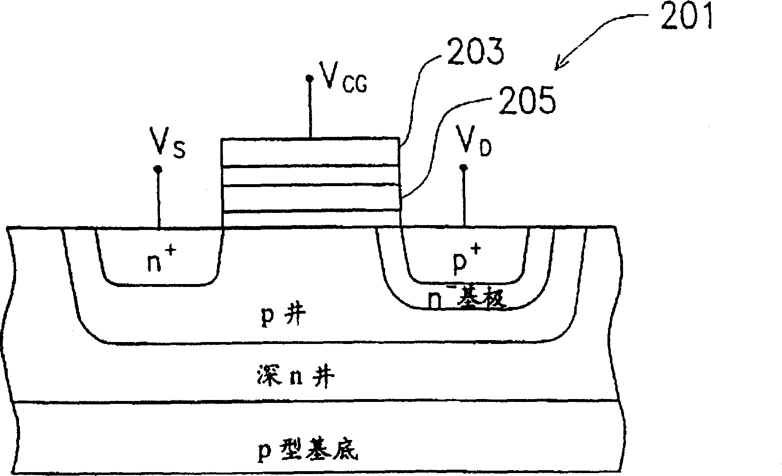
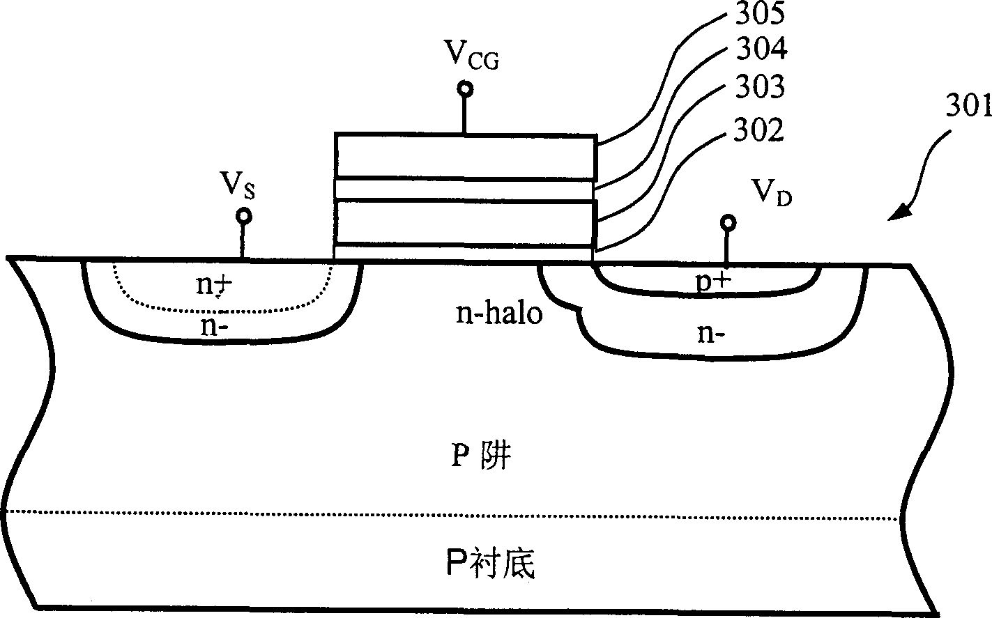
[0035] image 3 is a schematic cross-sectional view of a flash memory unit 301 on a p-type semiconductor substrate. It contains: a tunnel thin oxide layer 302 formed on the p-type semiconductor substrate; a stacked gate structure located on the tunnel thin oxide layer 302, the stacked gate structure includes a floating gate 303 and a control gate 305, The floating gate 303 and the control gate 305 are electrically isolated by a silicon dioxide / silicon nitride / silicon dioxide composite dielectric layer 304; a source region is formed in the first layer of the stacked gate structure composed of the floating gate 303 and the control gate 305. In the substrate at the edge, the source region includes a low-concentration phosphorus implanted n-source region located in the substrate at the first edge of the stacked gate structure and extending under the stacked gate structure, and a high An n+ source region implanted with arsenic concentration is located in the n-source region at the...


PUM

PropertyMeasurementUnit
Thicknessaaaaaaaaaa

Abstract

The flash storage unit includes a semi-conductor substrate of P type and P pit in the said substrate a includes a semi-conductor substrate of P type and P pit in the said substrate, a tunnelling the oxidation layer on the semi-conductor substrate, a stacked grid structure including floating grid and control grid of which floating grid is isolated to the control grid through the composite media layer of silica/silicon nitride/silica, on the tunnelling thin oxidation layer; a source region consisting of a n(-) source region injected by low concentration phosphorus and prolongated below the floating grid as well as a n(-) source region injected by high concentration arsenic, it the substrate of the first edge of the said stacked grid structure, a drain regino consisting of a n(-) drain regino injected by low concentration phosphorus.

Description

technical field [0001] A flash memory unit and a manufacturing method thereof belong to a flash memory and a manufacturing method thereof that utilize source-enhanced band tunneling hot electron injection to perform a write operation, and in particular relate to a manufacturing method of the drain region of the flash memory unit . Background technique [0002] The floating gate type non-volatile memory originated from the MIMIS (Metal-Insulator-Metal-Insulator-Semiconductor: Metal-Insulator-Metal-Insulator-Semiconductor) structure proposed by D. Kahng and S. Sze in 1967. It adds a metal floating gate and an ultra-thin tunnel oxide layer to the traditional MOSFET (Metal-Oxide-Semiconductor Field Effect Transistor: Metal-Oxide-Semiconductor Field Effect Transistor), and uses the floating gate to store charges. In 1984, Masuoka and others first proposed the concept of flash memory (Flash Memory), that is, by erasing and programming by bit and bit by block, the high speed of fl...

Claims


Application Information

Patent Timeline
IPC IPC(8): H01L21/8239H01L21/8246H01L27/10H01L27/112
Inventor 潘立阳朱钧
Owner TSINGHUA UNIV
Why Eureka
Try Eureka