Organic electroluminescent device of electroluminescent unit with lamina

A luminescent and organic field technology, applied in the field of organic electroluminescent devices, can solve the problems of not providing working examples, reducing the overall light output efficiency, and reducing luminous efficiency, and achieve the goal of improving luminous efficiency, increasing life, and increasing brightness Effect

Inactive Publication Date: 2003-08-27
GLOBAL OLED TECH
View PDF45 Cites 67 Cited by
  • Summary
  • Abstract
  • Description
  • Claims
  • Application Information

AI Technical Summary

Problems solved by technology

First, it requires complex wiring to address each OLED cell in the stack
Second, the electrode layers between the OLED cells in the stack absorb light and, if processed too thick, cause light loss which reduces overall light output efficiency
So-called transparent electrodes are known, but still absorb significant levels of light and are difficult to fabricate on organic structures
In fact, Burrows et al., with the aid of a mathematical model, explained the severe reduction in luminous efficiency caused by the expected light loss caused by the internal electrode layer
Third, if the electrodes are processed too thin for improved optical properties, the sheet resistance is too high, requiring high drive voltages for each individual OLED element, and non-uniform light emission across the device
Jones et al. suggested that the device structure could be used to produce OLED devices with higher luminous efficiency and higher operational stability, but did not provide working examples
Nor does Jones et al. suggest how to produce useful devices without the use of conductor layers

Method used


Image

  • Organic electroluminescent device of electroluminescent unit with lamina
  • Organic electroluminescent device of electroluminescent unit with lamina
  • Organic electroluminescent device of electroluminescent unit with lamina

Examples


Embodiment 1

[0206] Example 1 (conventional OLED-comparison):

[0207] A conventional non-stacked OLED was prepared as follows: a 1 mm thick glass substrate coated with a transparent ITO conductive layer was cleaned and dried using an industrial glass washer tool. The thickness of ITO is about 42 nm and the sheet resistance of ITO is about 68 Ω / square. The ITO surface was then treated with an oxidizing plasma to render the surface suitable as an anode. By decomposing CHF in an RF plasma processing chamber 3 gas, a CFx layer with a thickness of 1 nm was deposited on the purified ITO surface as a HIL. The substrate is then transferred to a vacuum deposition chamber for deposition of all other layers on top of the substrate. at about 10 -6 Under Torr vacuum, the following layers were deposited by sublimation from a heated boat in the following order:

[0208] (1) HTL, 75nm thick, composed of NPB;

[0209] (2) ETL (also used as emission layer), 60nm thick, composed of Alq;

[0210] (3) ...

Embodiment 2

[0213] Embodiment 2 (comparison)

[0214] A stacked OLED was fabricated with layers in the following order:

[0215] (1) HTL, 50nm thick, composed of NPB;

[0216] (2) ETL (also used as emission layer), 50nm thick, composed of Alq;

[0217] (3) Thin metal electrodes, 1nm thick, composed of Mg:Ag;

[0218] (4) Another thin metal electrode, 1.5nm thick, composed of Ag;

[0219] (5) HTL, 50nm thick, composed of NPB;

[0220] (6) ETL (also used as emission layer), 50nm thick, composed of Alq;

[0221] (7) Cathode, about 210nm thick, composed of Mg:Ag.

[0222] The processing steps were the same as in Example 1 except for the deposition of the layers described above. The stacked device structure is denoted as ITO / CFx / NPB(50) / Alq(50) / Mg:Ag / Ag / NPB(50) / Alq(50) / Mg:Ag.

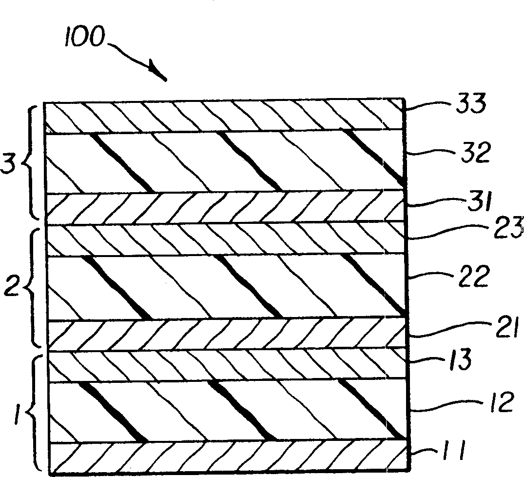
[0223] The stacked OLED requires a driving voltage of 21.2 V to pass 20mA / cm 2 . Its EL efficiency is 0.1cd / A. Its luminous efficiency-current characteristics, designated as Example 2, are shown in Image 6 ....

Embodiment 3

[0224] Embodiment 3 (comparison)

[0225] A stacked OLED was fabricated with layers in the following order:

[0226] (1) HTL, 75nm thick, composed of NPB;

[0227] (2) ETL (also used as emission layer), 60nm thick, composed of Alq;

[0228] (3) metal electrode, 10nm thick, made of Mg;

[0229] (4) HTL, 75nm thick, composed of NPB;

[0230] (5) ETL (also used as emission layer), 60nm thick, composed of Alq;

[0231] (6) Cathode, approximately 210nm thick, composed of Mg:Ag.

[0232] The processing steps were the same as in Example 1 except for the deposition of the layers described above. The stacked device structure is denoted as ITO / CFx / NPB(75) / Alq(60) / Mg / NPB(75) / AIq(60) / Mg:Ag.

[0233] The stacked OLED has a driving voltage of 11.2V and a current density of 20mA / cm 2 and EL efficiency of 1.3 cd / A. Its luminous efficiency-current characteristics, designated as Example 3, are shown in Image 6 .


PUM


Abstract

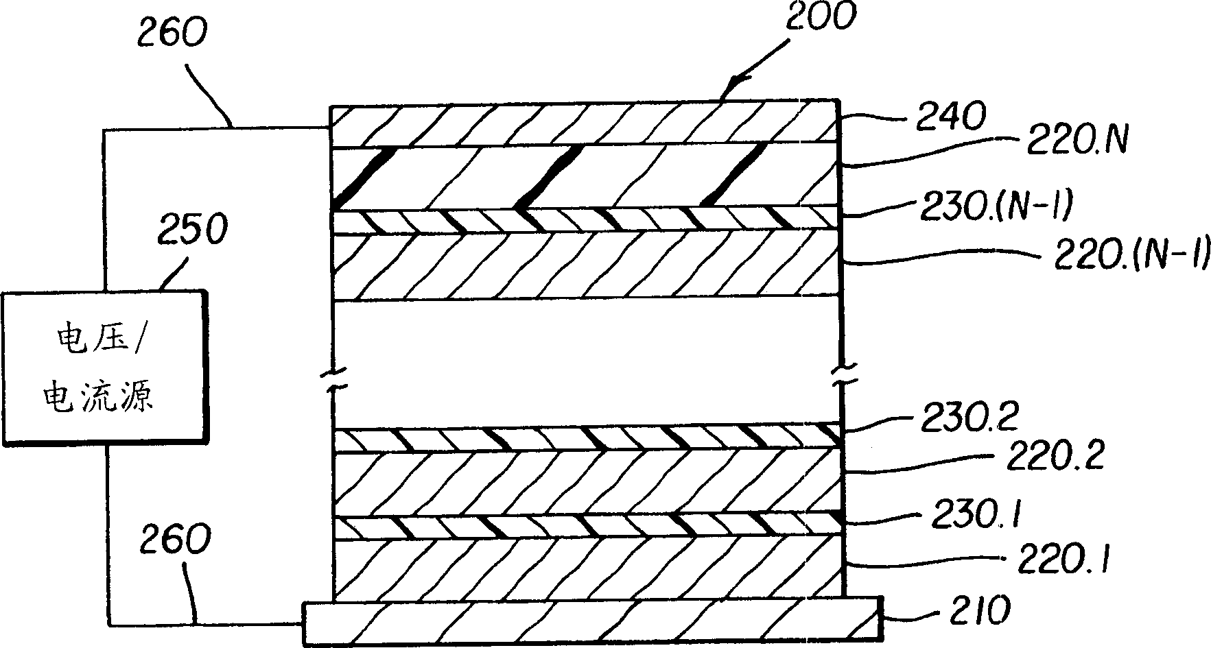
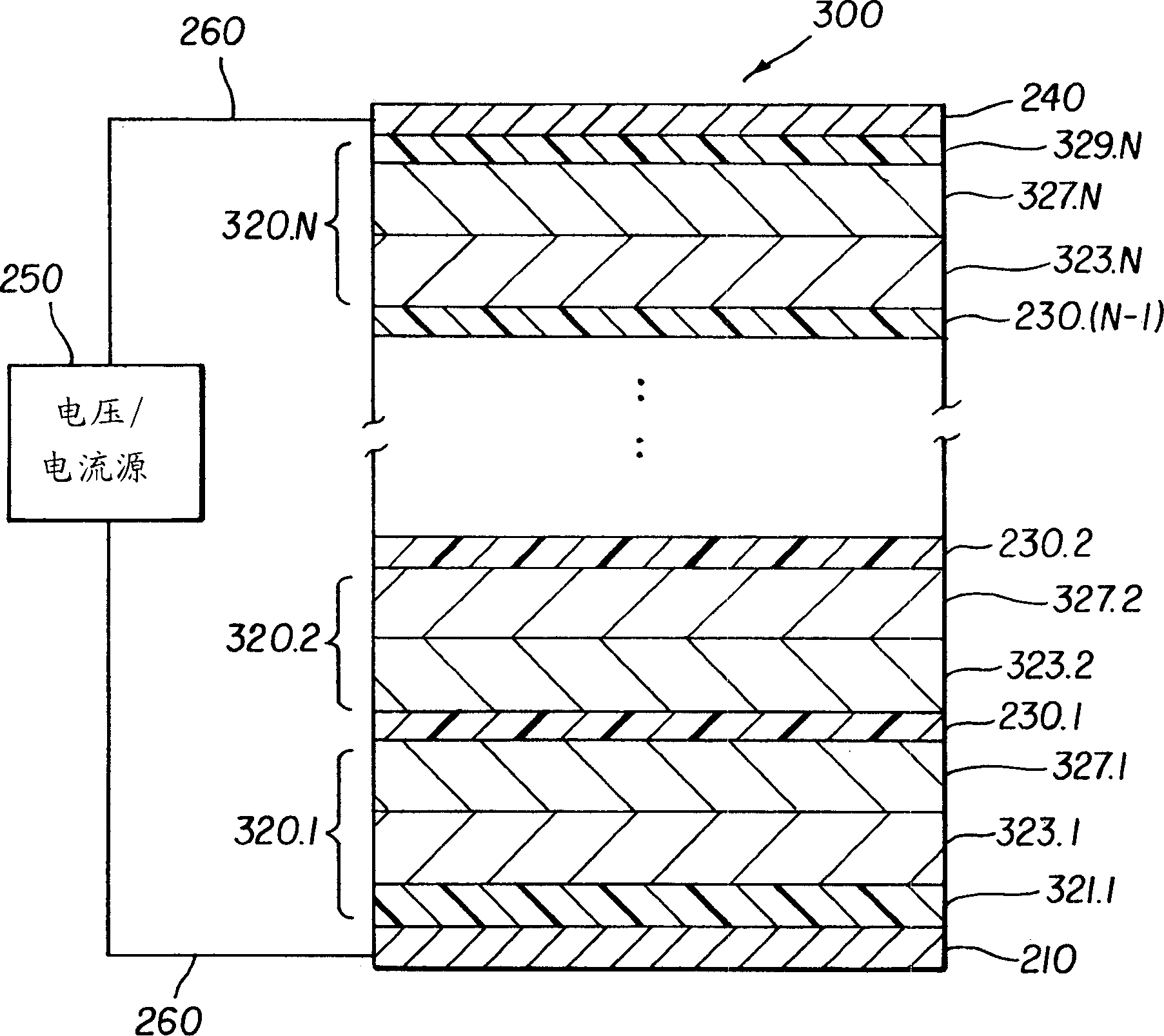
A stacked organic electroluminescent device and a method of making such device is disclosed. The device comprises an anode, a cathode, at least two organic electroluminescent units disposed between the anode and the cathode, and a doped organic connector disposed between each adjacent organic electroluminescent unit wherein the organic electroluminescent unit comprises at least one organic hole-transporting layer and one organic electron-transporting layer. The doped organic connector comprises at least one n-type doped organic layer or one p-type doped organic layer, or combinations of layers thereof.

Description

technical field [0001] The present invention relates to the provision of stacked organic electroluminescent units to form organic electroluminescent devices. Background technique [0002] Organic electroluminescent (EL) devices or organic light emitting diodes (OLEDs) are electronic devices that emit light in response to an applied electrical potential. The structure of an OLED sequentially includes an anode, an EL medium, and a cathode. An EL medium disposed between an anode and a cathode generally includes an organic hole transport layer (HTL) and an organic electron transport layer (ETL). In ETL, near the HTL interface, holes and electrons recombine and emit light. Tang et al. (Applied Physics Letters, 51, 913 (1987), Journal of Applied Physics, 65, 3610 (1989), and commonly assigned US-A-4,769,292) demonstrated high efficiency OLEDs using such layered structures. Thereafter, numerous OLEDs having various layered structures including polymer materials have been disclos...

Claims


Application Information

Patent Timeline
Patent Type & Authority Applications(China)
IPC IPC(8): H01L51/50H01L27/32H01L51/00H01L51/30H01L51/52H05B33/12H05B33/26
CPCH01L27/3244H01L51/0059Y10S428/917H01L51/0089H01L51/0085H01L51/0077H01L51/0052H01L27/322H01L51/0084H01L27/3281H01L51/5036H01L51/0062H01L51/5278H01L2251/5361H05B33/0896H01L51/5016H01L27/3211Y10T428/26H05B45/60Y02B20/30H10K59/35H10K59/38H10K85/649H10K85/615H10K85/631H10K85/30H10K85/341H10K85/351H10K85/342H10K50/125H10K50/11H10K2101/10H10K50/19H05B33/26H10K59/12H10K59/17
Inventor L·-S·L·廖C·W·邓
Owner GLOBAL OLED TECH
Why Eureka
Try Eureka