Upholder with multiple materials layers in field emission flat panel displays
A flat-panel display device and field emission technology, applied in electroluminescent light sources, instruments, electrical components, etc., can solve problems such as troublesome operation, difficult application, and time-consuming
- Summary
- Abstract
- Description
- Claims
- Application Information
AI Technical Summary
Problems solved by technology
Method used
Image
Examples
Embodiment Construction
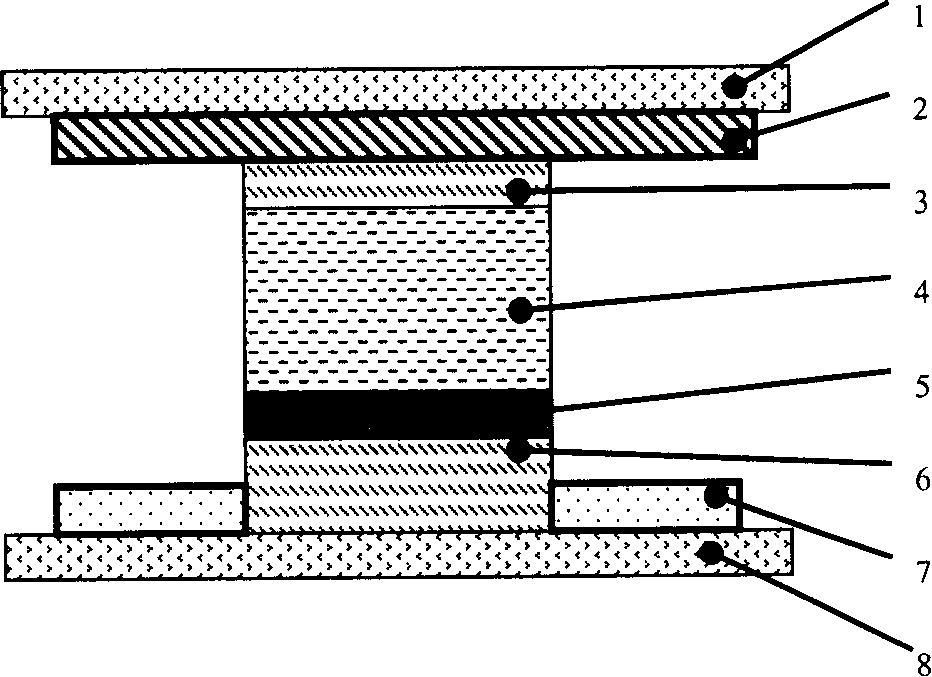
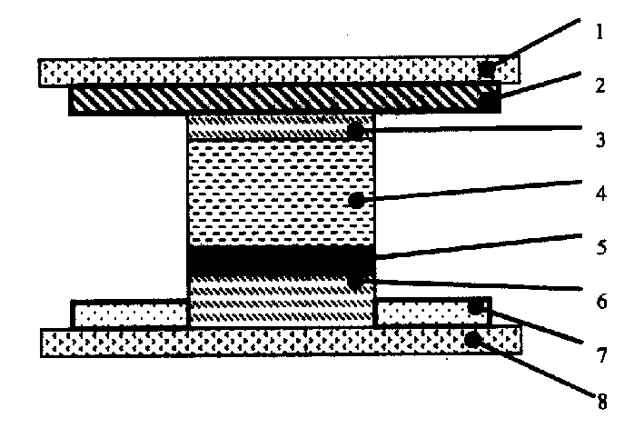
[0014] Such as figure 1 As shown, a better support is needed between the anode substrate 8 and the cathode substrate 1 of the field emission display device. The best embodiment of the present invention is a support formed by multiple functional material layers, namely the insulating layer 6, the black matrix material layer 5, the getter material layer 4 and the insulating layer 3 overlapped in sequence, first in the anode strip 7 gaps A layer of insulating layer 6 is formed by coating, printing, coating or template method, which can be aluminum oxide, silicon dioxide, tantalum pentoxide, etc., so as to avoid short circuit or leakage between the black matrix material layer 5 and the anode strip. Then, print or coat a layer of black matrix material layer 5 on it, which can be graphite milk, etc., to eliminate the glare of the screen and improve the display contrast of the screen. The third layer of material layer is a non-evaporable getter material Layer 4, can be zirconium, va...
PUM
 Abstract
Description
Claims
Application Information

