Multi-quantum well waveguide butt coupling method

A multi-quantum well and docking coupling technology, which is applied in the coupling of optical waveguides, phonon exciters, semiconductor lasers, etc., can solve the problems of reduced coupling efficiency of multi-quantum well waveguides, affecting the performance of integrated devices, and difficult to guarantee material quality. Achieve the effects of improving stacking bending phenomenon, having universal applicability, and reducing light loss

Inactive Publication Date: 2003-12-31
INST OF SEMICONDUCTORS - CHINESE ACAD OF SCI
View PDF0 Cites 12 Cited by
  • Summary
  • Abstract
  • Description
  • Claims
  • Application Information

AI Technical Summary

Problems solved by technology

However, due to the enhancement effect of the edge of the dielectric film when epitaxy is selected, the regrown multiple quantum wells at the interface will bend and pile up, the quality of the material is difficult to guarantee, and large li

Method used


Image

  • Multi-quantum well waveguide butt coupling method
  • Multi-quantum well waveguide butt coupling method
  • Multi-quantum well waveguide butt coupling method

Examples


Embodiment

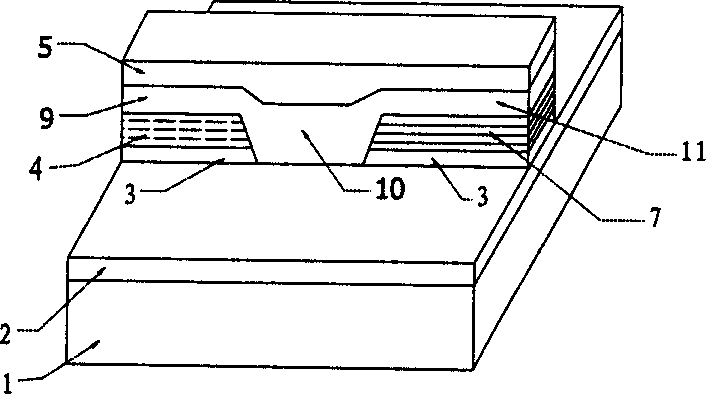
[0037] Figure 4 It is a schematic diagram of the EML structure made by the waveguide butt coupling method. The specific production process is as follows:

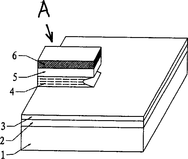
[0038] 1. On the (100) surface of n-type indium phosphide (InP) substrate 1, the optimally designed laser multi-quantum well active structure is epitaxially grown, specifically including the lower waveguide layer 2, the InP etch stop layer 3 (with a thickness of 10 -50nm), multiple quantum well (MQW) 4, upper waveguide 5 and InP capping layer 6;

[0039] 2. Deposit a layer of silicon dioxide (SiO2) with a thickness of about 100 nm by thermal oxidation CVD 2 ) Dielectric film, the mask photolithography out the laser table bar (see figure 1 ), the strip width is 10-50um, the strip length is 200-800um, the etching stops at the InP barrier layer 3, and the laser bar end side drills deeper;

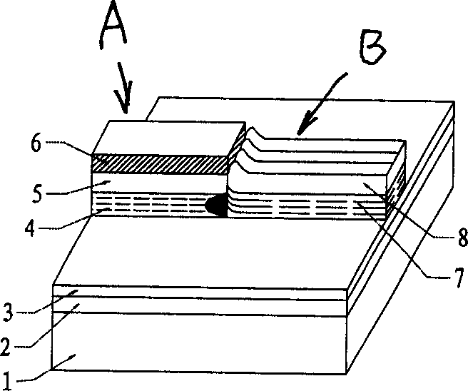
[0040] 3. Epitaxial growth modulator active structure (MD-MQW), because silicon dioxide (SiO 2 ) Dielectric film cannot grow crystal...


PUM

PropertyMeasurementUnit
Thicknessaaaaaaaaaa
Thicknessaaaaaaaaaa

Abstract

The invention discloses a multiple quantum well wave-guide end-to-end coupling process comprising, (1) epitaxially growing the multiple quantum well structure of the device A on the substrate, (2) depositing a layer of dielectric-coating, and mask photo-etching, etching the multiple quantum structure besides the A strips, (3) epitaxially growing the multiple quantum well structure of the device B, (4) mask photo-etching the less satisfying growing quality portion of the A and B interface. (5) extending optimization of the designed body material to the larger area, to serve simultaneously as both the up waveguide of device A and B, and the coupling waveguide between them. The process of the invention may be used to eliminate the inanity and multiple quantum well bending caused by direct linkage, to lower coupling loss and to increase optical output power. The invention can be applied to the making of a plurality of photoelectron integrated device.

Description

technical field [0001] The invention relates to a waveguide docking coupling method, in particular to a multi-quantum well waveguide docking in an optoelectronic integrated device (such as a laser, a modulator, an optical amplifier, a filter, and a wavelength converter whose active region is a multi-quantum well) Coupling method. Background technique [0002] To make integrated optoelectronic devices, an important issue is to make low-loss optical channels, so that optical butt coupling can be effectively realized between different components on the same substrate. At present, the optoelectronic monolithic integrated production technology mainly has the following methods: [0003] 1) Selected area growing (SAG) method, see IEEE J. Quantum Electron., Vol. 29, 1993, pp. 2088-2096 and Electron. Lett., Vol. 32, 1996, pp. 109-111). This technology uses a dielectric mask to accelerate the growth of quantum wells in some areas, and achieves the purpose of growing the quantum well...

Claims


Application Information

Patent Timeline
IPC IPC(8): G02B6/42H01S5/026
Inventor 胡小华王圩朱洪亮
Owner INST OF SEMICONDUCTORS - CHINESE ACAD OF SCI
Why Eureka
Try Eureka