Wide-band low-loss semiconductor saturable absorbing mirror for mode-locking laser

A saturable absorption, mode-locked laser technology, applied in the field of broadband low-loss semiconductor saturable absorption mirrors, can solve the problems of low output power, large loss of saturable absorption mirrors, and high threshold of mode-locked lasers, and achieve the effect of narrow pulse width

Inactive Publication Date: 2004-02-25
TIANJIN UNIV
View PDF0 Cites 2 Cited by
  • Summary
  • Abstract
  • Description
  • Claims
  • Application Information

AI Technical Summary

Problems solved by technology

However, the reflectivity of the mirror directly coated with metal film can reach 98% in theory,

Method used


Image

  • Wide-band low-loss semiconductor saturable absorbing mirror for mode-locking laser
  • Wide-band low-loss semiconductor saturable absorbing mirror for mode-locking laser
  • Wide-band low-loss semiconductor saturable absorbing mirror for mode-locking laser

Examples


Embodiment Construction

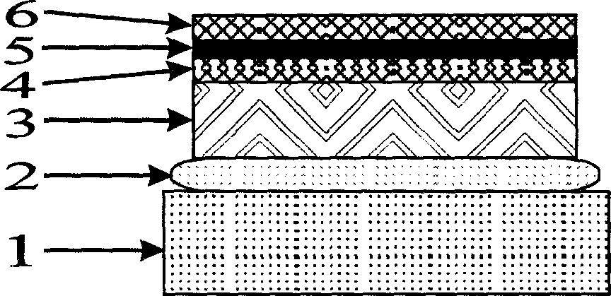
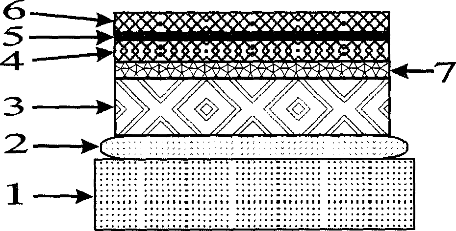
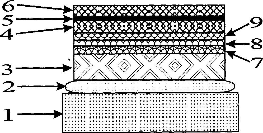
[0016] image 3 It is a schematic diagram of the vertical cross-section structure of a semiconductor saturable absorbing mirror inserted into a transparent medium layer and a high-reflection film designed according to the present invention. For the sake of brevity in describing the fabrication process, the supporting substrate is temporarily ignored. And only take the fabrication of a broadband semiconductor saturable absorber mirror with a central wavelength of 800 nanometers as an example for illustration.

[0017] [1] The saturable absorber 5 is an InGaAs quantum well. grown on a lattice-matched GaAs substrate. In order to make the quantum well at the peak of the standing wave field of the film system, transparent semiconductor materials AlGaAs4 and 6 are used as transition layers. In order to ensure the smoothness and uniformity of the semiconductor surface after etching, a selective etching method must be used, that is, a stop layer is required, and the material of the...


PUM


Abstract

The present invention discloses a wideband low-loss semiconductor saturable absorption lens for mode-locking laser. Said absorption lens is successively formed from reflector supporting piece, adhesive layer, metal (gold or siler) film reflecting layer, transparent semiconductor layer (aluminum gallium arsenide and indium aluminium gallium arsenide), semiconductor quantum well saturable absorbent(gallium arsenide, indium gallium arsenide) and transparent semiconductor layer (aluminum gallium arsenide and indium aluminum gallium arsenide). Between the metal film reflecting layer and adjacent transparent semiconductor layer a transparent medium layer with low refractive index (less than 1.65) can be inserted or between said transparent medium layer and transparent semiconductor layer a high reflecting film layer formed from high-low refractive index medium layer pair can be more inserted.

Description

technical field [0001] The invention relates to a broadband low-loss semiconductor saturable absorber mirror for mode-locked lasers. It is an auxiliary technology for mode-locked lasers. Background technique [0002] A saturable absorber acts as a pure absorber for low-energy incident light, while for high-energy incident light, it becomes transparent due to the saturation of the absorption capacity. When such a substance is placed in the resonant cavity, the loss of continuous light with small energy in the cavity increases, while the loss of high-energy pulses becomes smaller, so it plays a role in selecting and shaping the pulse and promotes pulse generation. It is an application in mode-locked lasers. of a technique. In the visible and near-infrared wavelength domains, suitable materials for fabricating saturable absorbers are semiconductors. The structure of the conventional broadband semiconductor saturable absorbing mirror (R. Fluck et al....

Claims


Application Information

Patent Timeline
IPC IPC(8): H01S3/02H01S3/098H01S5/065
Inventor 张志刚王清月柴路孙大睿赵江山刘永军
Owner TIANJIN UNIV
Why Eureka
Try Eureka