Supercharge Your Innovation With Domain-Expert AI Agents!

Reflector utilizing microimage to make exposure and its production method

A manufacturing method and mirror technology, applied in the field of reflective optical mirrors, can solve the problems of different values ​​of etching rates on the surface of silicon oxide, and achieve the effect of good optical properties

Inactive Publication Date: 2004-05-12
INFINEON TECH AG
View PDF0 Cites 0 Cited by
  • Summary
  • Abstract
  • Description
  • Claims
  • Application Information

AI Technical Summary

Problems solved by technology

[0007] The problem of inhomogeneous layer thicknesses of native oxides can theoretically be countered by controlled etchback of the resulting oxide layer, but the etching step is also subject to statistical fluctuations, and as a result the etch rate on silicon oxide surfaces may vary different values

Method used


Image

  • Reflector utilizing microimage to make exposure and its production method
  • Reflector utilizing microimage to make exposure and its production method
  • Reflector utilizing microimage to make exposure and its production method

Examples


Embodiment Construction

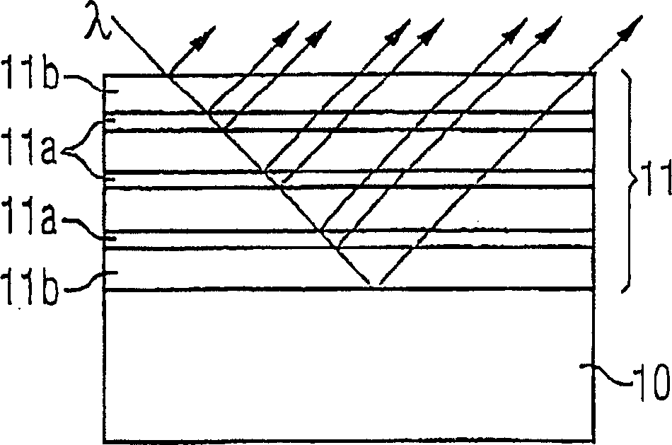
[0028] Figure 1A mirror is shown comprising a substrate 10 and a succession of thin layers 11a, 11b deposited one on top of the other. A semiconductor substrate or any other sufficiently thick and defined substrate can be used as the substrate 10. The layer thicknesses of the individual layers 11a and 11b are dimensioned such that the wavelength λ can be reflected at the layer interfaces adjacent to each other in such a way that the reflected partial light beams interfere structurally with each other; the highest possible light intensity of the total reflected radiation is at the semiconductor A short exposure time of the article is desired. The large angle of incidence of electromagnetic radiation having wavelength λ is shown in the figure, if Figure 1 Reflection at the non-non-interface is for illustration only; in practice, the reflection actually occurs perpendicular to the surface of the multilayer structure 11 .

[0029] exist Figure 1 The layered sequence 11 is prod...


PUM

PropertyMeasurementUnit
coating thicknessaaaaaaaaaa

Abstract

A reflective optical mirror for semiconductor fabrication includes a capping layer above a reflective multilayer sequence. A doping is provided for the capping layer and an artificial oxide layer is grown on the capping layer with the aid of hydrogen peroxide, in particular in the presence of a catalyst. The artificially grown oxide layer is more homogeneous than a naturally grown oxide and thereby improves optical properties of the mirror during a lithographic exposure of semiconductor products.

Description

technical field [0001] The invention relates to a mirror for the lithographic exposure of a semiconductor product, in which a multilayer structure is formed on a substrate and, on top of the multilayer structure, a covering layer of material - a natural oxide layer in air generated on it. The present invention further relates to the reflective optical mirror according to the above-mentioned item 9 of the patent scope of the application. Background technique [0002] In semiconductor manufacturing, the surface of a semiconductor substrate or the surface of thin layers arranged thereon is lithographically scribed by means of a light-resistant layer deposited on the surface and lithographically exposed. During lithographic exposure, a two-dimensional masking structure is developed onto the photoresist layer. The carrier of the shielding structure is the so-called reticle, which is also called a mask here. On this reticle, the exposed structures are realized in the form of a ...

Claims


Application Information

Patent Timeline
Patent Type & Authority Applications(China)
IPC IPC(8): G02B1/02G02B1/10G02B1/12G02B5/08G03F1/24G03F7/00G03F7/20G06F13/28
CPCB82Y10/00G03F7/70958G03F1/24B82Y40/00
Inventor F·-M·卡姆J·劳
Owner INFINEON TECH AG
Features
  • R&D
  • Intellectual Property
  • Life Sciences
  • Materials
  • Tech Scout
  • Unparalleled Data Quality
  • Higher Quality Content
  • 60% Fewer Hallucinations
Learn More