Opto-electronic device integration

A device and electronic chip technology, applied in the field of optoelectronic device integration

Inactive Publication Date: 2004-08-18
CUFER ASSET LTD LLC
View PDF0 Cites 6 Cited by
  • Summary
  • Abstract
  • Description
  • Claims
  • Application Information

AI Technical Summary

Problems solved by technology

[0024] What is lacking in the prior art is a solution that eliminates the need to pattern the protective layer on the laser while allowing anti-reflection coating to be applied over the entire wafer (i.e. laser and detector)

Method used


Image

  • Opto-electronic device integration
  • Opto-electronic device integration
  • Opto-electronic device integration

Examples


Embodiment Construction

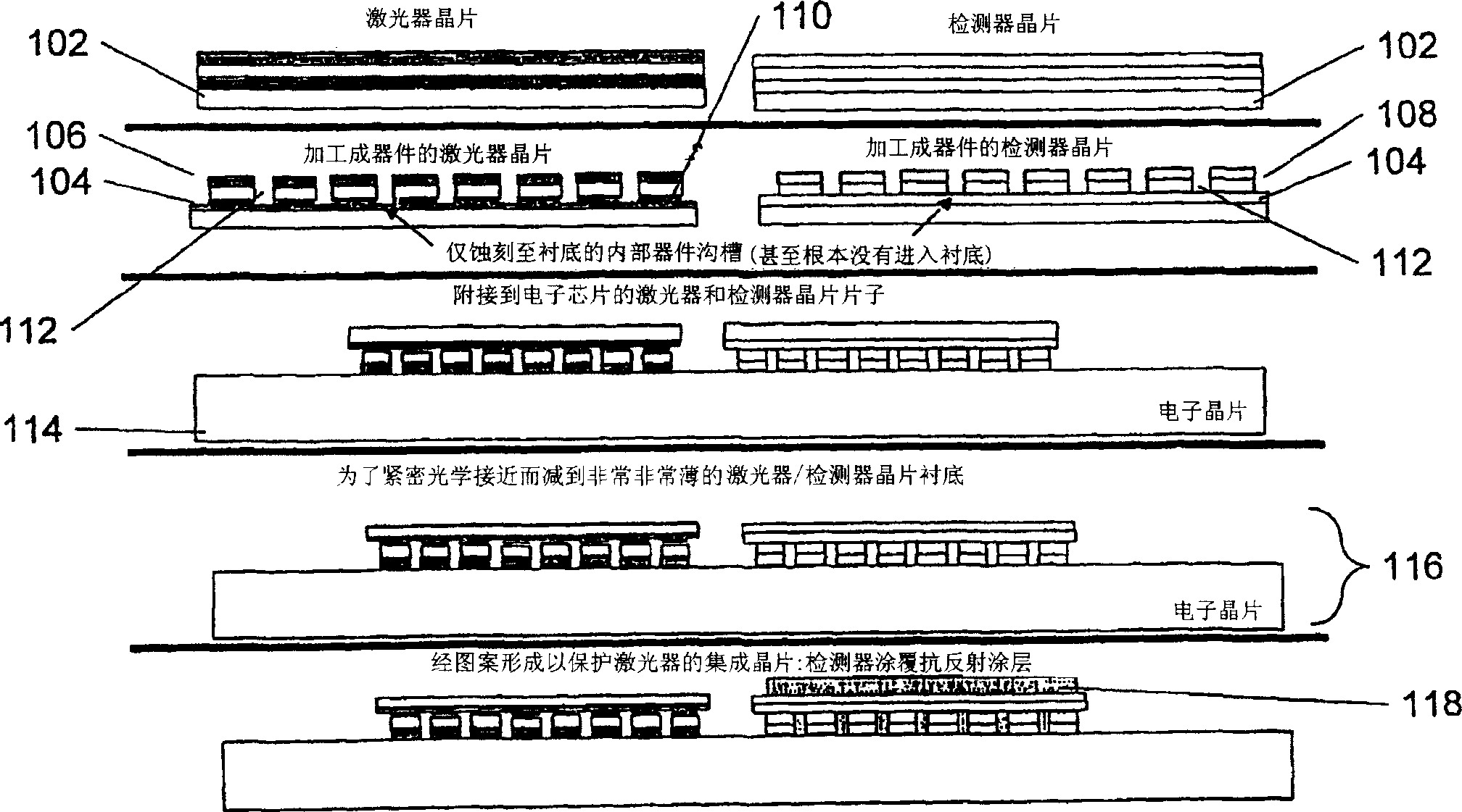
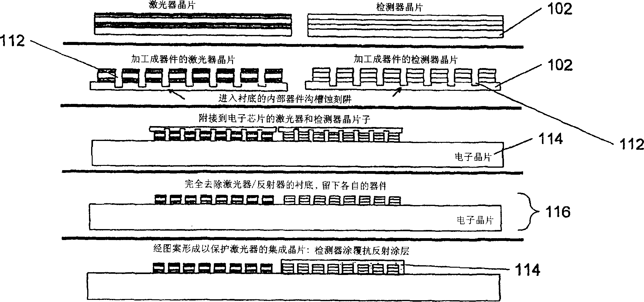
[0065] Figure 5 An exemplary method in accordance with the techniques of the present invention is illustrated at a simplified high-level overview. This process allows close optical proximity, eliminates absorbing regions, provides higher structural integrity, and has better heat dissipation characteristics while overcoming the disadvantages of the prior art.

[0066] exist Figure 5 In this method, laser wafer 502 (consisting of lasers integrated with substrate 102) or detector wafer 504 (consisting of detectors integrated with substrate 102) is obtained using conventional techniques or purchased from some third party. device configuration). Alternatively, hybrid chips consisting of lasers and detectors integrated on a common substrate in some pattern or grouping can also be manufactured or purchased.

[0067] The etched trenches 506 process a wafer into individual discrete devices (by etching into the substrate) or in some cases into groups of suitable devices, e.g. What...


PUM


Abstract

A method of creating a hybridized chip having at least one top active device coupled to an electronic chip where a top active device is combined with an electronic chip having electronic chip contacts, when at least some of the top active device contacts are not aligned with at least some of the electronic chip contacts, and each of the at least some top active device contacts has an electrically corresponding electronic chip contact. The method involves creating sidewalls defining openings in the substrate, extending from the first side at the active device contacts to the bottom fo the substrate opposite the first side, at points substantially coincident with the active device contacts; making the sidewalls electrically conductive; and connectin g the points and the electronic chip contacts with an electrically conductive material.

Description

technical field [0001] The invention relates to the integration of optoelectronic devices, especially the integration of high yield and high density optoelectronic devices. Background technique [0002] figure 1 and figure 2 A method employed in the prior art to attach multiple bottom emitting (or detecting) devices (also referred to as back emitting or detecting devices) to form an integrated optoelectronic device is described. [0003] according to figure 1 In the method, a plurality of lasers are formed on the wafer substrate 102 in a conventional manner, and for a plurality of detectors (referred to interchangeably as photodetectors here), on its own or on the same wafer substrate as the lasers, the method also Same. Generally speaking, the portion 104 of the substrate 102 closest to the connection between the optoelectronic devices 106, 108 and the substrate 102 is made of a material that is optically transparent to the operating wavelen...

Claims


Application Information

Patent Timeline
Patent Type & Authority Applications(China)
IPC IPC(8): G02B6/42H01L21/68H01L25/16H01L27/144H01L27/15H01S5/02H01S5/02375H01S5/40H01S5/42
CPCG02B6/4292H01L24/95H01S5/0201H01S5/0224G02B6/4204H01S5/423H01L2221/68359H01S5/02268H01S5/0217H01S5/4087H01L2924/0002H01L27/156H01S5/02276H01S5/02272G02B6/4249H01L25/167H01L21/6835H01L2221/68363H01L27/144H01L2924/01322H01L2924/351H01L2924/12042H01S5/02375H01S5/0234H01S5/0237H01S5/02345H01L2924/00H01L31/10
Inventor 格雷格·杜德夫约翰·特雷泽
Owner CUFER ASSET LTD LLC
Why Eureka
Try Eureka