


Quick Research
Generate reliable direction feasibility study reports for your R&D in just a few steps.

Technical Q&A
Discover and master advanced knowledge NOW. Basics, ideas, possibilities, all at once.

Find Solutions
As an expert in R&D theories, this can generate solutions to your technical problems instantly.

Evaluate Feasibility
Analyze your overall solution with one click, know your potential R&D risks in advance.

Monitor Landscape
Get weekly tech updates, stay abreast of the latest tech innovations and key insights.
Method for producing biological protein molecular chips
A manufacturing method and protein technology, applied in the field of biosensing, can solve the problem of low integration, and achieve the effect of improving the firmness and ensuring the activity
- Summary
- Abstract
- Description
- Claims
- Application Information
AI Technical Summary
Problems solved by technology
Method used
Image

Examples
Embodiment 1
[0018] Embodiment 1: the concrete processing steps of the present invention are as follows:
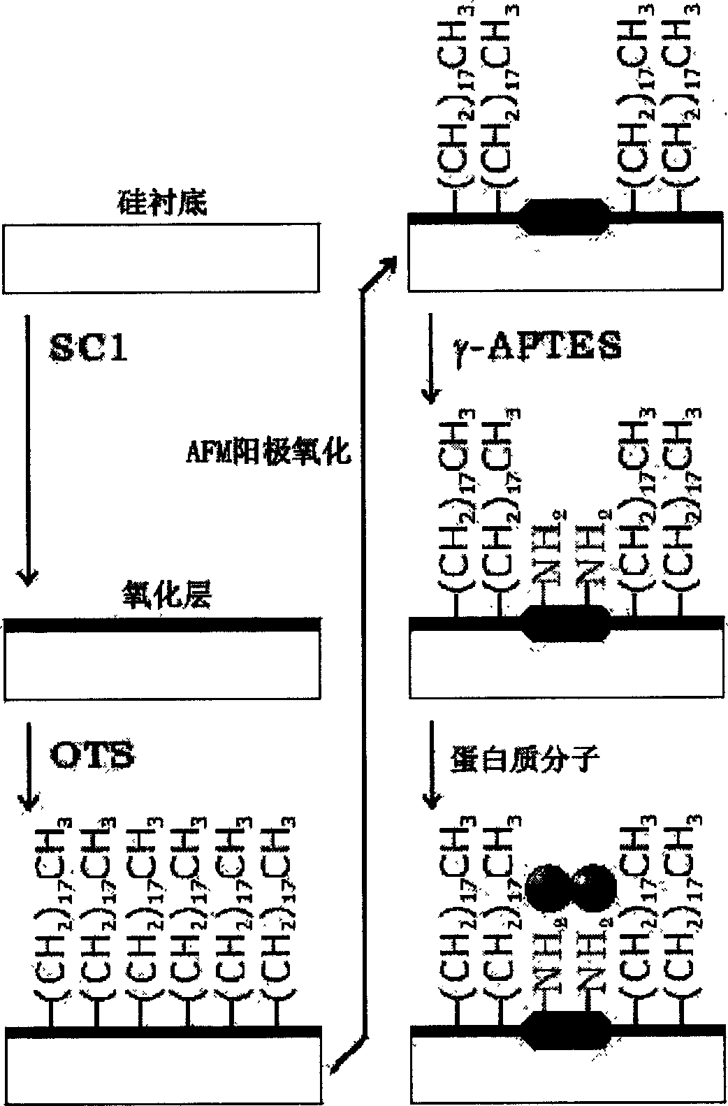
[0019] a. First, standard semiconductor technology is used to clean and thermally oxidize the silicon wafer; the surface of the cleaned and thermally oxidized silicon wafer has a layer of 500 nanometer silicon dioxide layer;
[0020] b. immerse the above-mentioned pretreated silicon chip in octadecyltrichlorosilane (OTS) for 10 minutes, so that the surface of the silicon chip has octadecyl groups, and octadecyl groups have repellency to protein molecules;
[0021] c. Adopt atomic force microscope (AFM) nano-etching technology to etch nano-patterns on the above-mentioned processed silicon wafer surface; the etching method is: apply a voltage between the atomic force microscope probe and the silicon surface, so that Atoms are oxidized into silicon dioxide; the probe is moved, etched into a square array with a side length of 50 nanometers, and the surface octadecyl group where the etched...
Embodiment 2
[0024] Embodiment two: the concrete processing steps of the present invention are as follows:
[0025] a. First, standard semiconductor technology is used to clean and thermally oxidize the silicon wafer; there is a silicon dioxide layer of 800 nanometers on the surface of the cleaned and thermally oxidized silicon wafer;
[0026] b. immerse the above-mentioned pretreated silicon chip in octadecyltrichlorosilane (OTS) for 10 minutes, so that the surface of the silicon chip has octadecyl groups, and octadecyl groups have repellency to protein molecules;
[0027] c. Adopt atomic force microscope (AFM) nano-etching technology to etch nano-patterns on the above-mentioned processed silicon wafer surface; the etching method is: apply a voltage between the atomic force microscope probe and the silicon surface, so that Atoms are oxidized into silicon dioxide; the probe is moved and etched into concentric circles with a radius of 200 nanometers and 400 nanometers and a line width of 50...
PUM
| Property | Measurement | Unit |
|---|---|---|
| radius | aaaaa | aaaaa |
| width | aaaaa | aaaaa |
Abstract
Description
Claims
Application Information
 - R&D Engineer
- R&D Manager
- IP Professional
- Industry Leading Data Capabilities
- Powerful AI technology
- Patent DNA Extraction
Browse by: Latest US Patents, China's latest patents, Technical Efficacy Thesaurus, Application Domain, Technology Topic, Popular Technical Reports.
© 2024 PatSnap. All rights reserved.Legal|Privacy policy|Modern Slavery Act Transparency Statement|Sitemap|About US| Contact US: help@patsnap.com