Multilayer device and its producing method
A device and component technology, applied in the field of packaging solutions for monolithic integrated systems, can solve problems such as unusable devices and incompatibility, and achieve the effect of improving reliability and quality
- Summary
- Abstract
- Description
- Claims
- Application Information
AI Technical Summary
Problems solved by technology
Method used
Image

Examples
Embodiment Construction
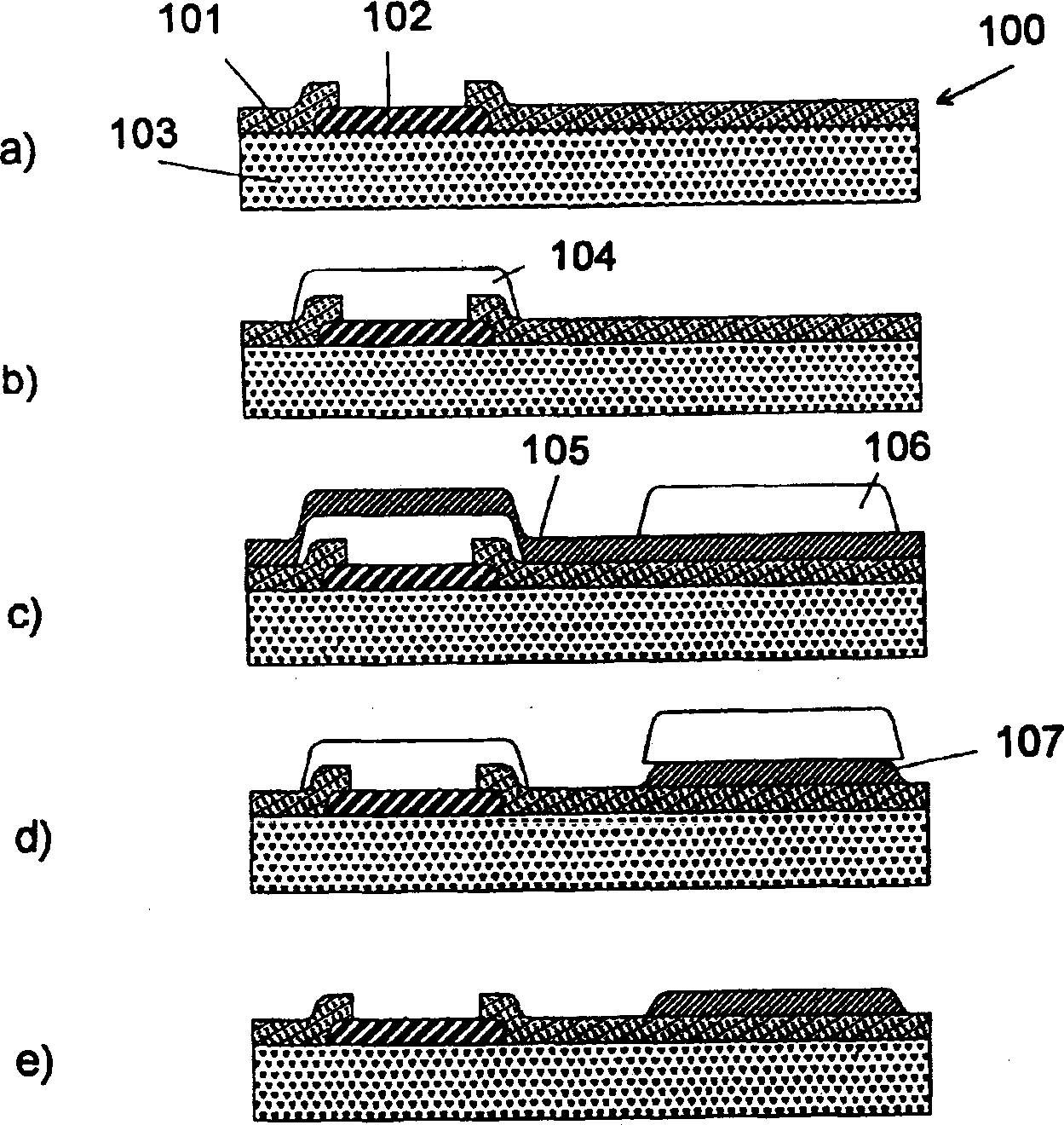
[0036] figure 1 a) shows a cross-sectional view of a preprocessed silicon wafer 100 . The passivation layer 101 may consist of a first layer of phosphosilicate glass (PSG) plus a layer of silicon nitride (SiN) - other combinations may also be used. Post-processing may include patterning of the layers in the passivation layer individually or simultaneously. Factors governing this process will be cost and technical issues such as the ease or feasibility of contamination control and reprocessing. The main function of the passivation layer is to prevent sodium contamination of the underlying circuitry. Aluminum contact pads 102 are shown, but the underlying conductive and dielectric layers are not included to improve the clarity of the drawing. A passivation layer 101 and a contact pad 102 are formed on a substrate 103 .
[0037] The first process steps carried out on the wafer 100, such as figure 1 Shown in b) is the deposition of the first layer of positive photoresist 104 ...
PUM
 Abstract
Description
Claims
Application Information