Operation method of non-volatile memory unit array
A non-volatile memory and memory cell technology, applied in the field of non-volatile memory cell arrays, can solve the problems of low programming efficiency, shrinking device size, and reducing reliability of electronic devices, etc.
- Summary
- Abstract
- Description
- Claims
- Application Information
AI Technical Summary
Problems solved by technology
Method used
Image
Examples
Embodiment Construction
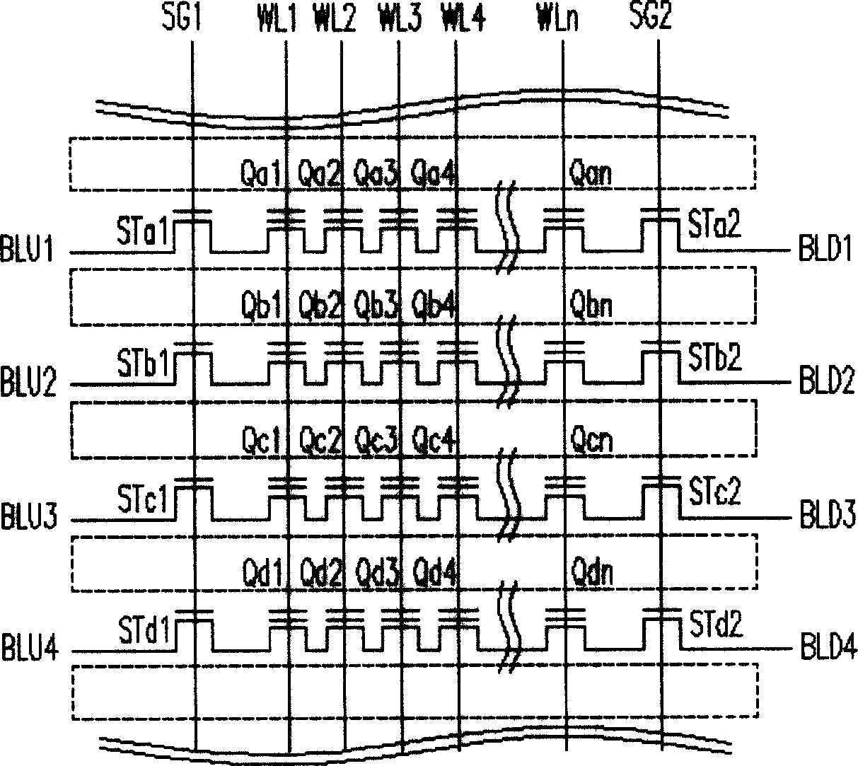
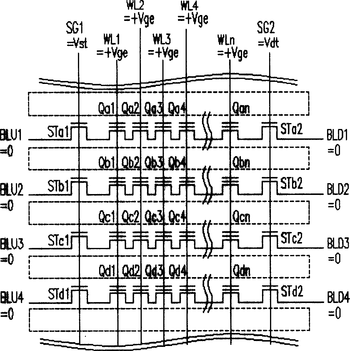
[0034] figure 1 A schematic circuit diagram of a non-volatile memory cell array is shown. Wherein, the non-volatile memory cell array is a NAND (NAND gate) array. However, the operation method of the non-volatile memory cell array of the present invention is suitable for NAND (NAND gate) type array. In this embodiment, 4 columns of NAND column memory cells are taken as an example for illustration.
[0035] Please refer to figure 1 The non-volatile memory cell array includes a plurality of select transistors STa1 - STd1 and STa2 - STd2 , a plurality of memory cells Qa1 - Qdn, a plurality of word lines WL1 - WLn, and select gate lines SG1 and SG2. The upper bit lines BLU1-BLU4 and the lower bit lines BLD1-BLD4.
[0036]The memory cells Qa1 to Qan form memory cell columns in the column direction, and are connected in series between the selection transistor STa1 and the selection transistor STa2 . The memory cells Qb1 to Qbn form memory cell columns in the column direction, a...
PUM
 Abstract
Description
Claims
Application Information


