A electron beam chemical amplitude positive resist and method for making same and photoetching technology

A chemical amplification and positive resist technology, which is applied to the photolithography process of the pattern surface, the photolithography exposure device, and the microlithography exposure equipment, etc., which can solve the problems such as difficult start

Inactive Publication Date: 2004-11-17
WUXI RES & DESIGN INST OF CHEM IND
View PDF0 Cites 1 Cited by
  • Summary
  • Abstract
  • Description
  • Claims
  • Application Information

AI Technical Summary

Problems solved by technology

[0008] In China, the development of "electron beam chemi...

Method used


Image

  • A electron beam chemical amplitude positive resist and method for making same and photoetching technology

Examples


Embodiment 1

[0047] Synthesis of host resin copolymer P(MMA-TBMA-MAA-IBMA)

[0048] In a 500ml four-necked flask, add purified MMA20g (0.2mol), MAA8.6g (0.1mol), TBMA21.3g (0.15mol), IBMA11.1g (0.05mol), then add THF150g, AIBN0.2g, pass Inject nitrogen, start stirring, control the reaction temperature to 65°C, and react for 24 hours. Pour the reactant into 1000ml cyclohexane for precipitation, suction filtration, take out the filter cake and dissolve it in 150ml THF, then precipitate it in 1000ml cyclohexane, suction filtration, repeat three times, then put the filter cake into a vacuum drying oven , baked at 60°C for 24 hours to obtain 38g of the main resin copolymer P(MMA-TBMA-MAA-IBMA).

Embodiment 2

[0050] Synthesis of host resin copolymer P(MMA-TBMA-MAA-IBMA)

[0051] The operation steps are the same as in Example 1, but the feeding amounts of MMA, MAA, TBMA, and IBMA are respectively 20g, 4.3g, 21.3g, and 22.2g to obtain 39.2g of the main resin copolymer P (MMA-TBMA-MAA-IBMA).

Embodiment 3

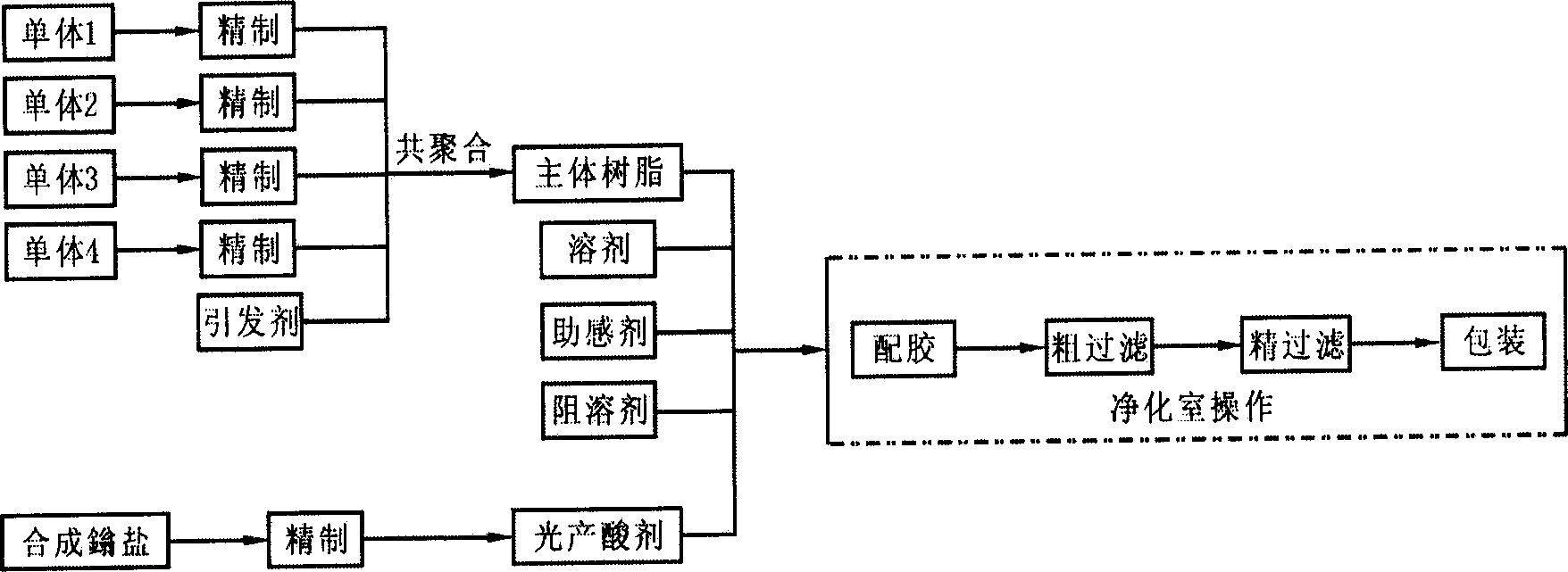
[0053] Compounding Technology of Electron Beam Chemically Amplified Positive Resist

[0054] Get the copolymer resin 13g of embodiment 1, add solvent ethylene glycol ethyl ether acetate 86g, photoacid generator diphenyl iodine trifluoromethanesulfonate 0.5g, synesthesia agent 2,4-dimethoxybenzoic acid 0.1 g and 0.5 g of tert-butyl cholate, a solvent-repelling solvent, were stirred and dissolved, and then filtered with a 0.1 μm filter membrane to obtain an electron beam chemically amplified positive resist.


PUM


Abstract

The invention is a kind of electron beam chemical amplifies positive slushing compound and the manufacturing method, and the etching process. The invention uses P (MMA-TBMA-MAA-IBMA) as the primary resin, the slushing compound belongs to the positive one with high resolution performance, or positive glue. The invention provides the synthesis of the primary resin, the synthesis of optical acid generating agent dibenzio-triflumidatemethyl petroleum sulfonate, the prescription and manufacturing method of the slughing compound. The resolution is 0.13ª–m, the sensitivity is 5-10ª–C/cm2 (50kV), reaches or approaches the international level.

Description

technical field [0001] An electron beam chemically amplified positive resist and its preparation method and photolithography process, specifically related to P (MMA-TBMA-MAA-IBMA) as the main resin, the resist is a positive resist with high resolution performance Resist, or positive resist. Background technique [0002] With the research and development of high-integration, ultra-high-speed, and ultra-high-frequency integrated circuits and devices, the feature size of large-scale integrated circuits and ultra-large-scale integrated circuits is becoming smaller and smaller, and the processing size enters deep submicron hundreds of nanometers or even nanometers. In the field of microelectronics technology, microfabrication technology (lithography technology) is the highest precision processing technology that humans can achieve so far. Therefore, each generation of integrated circuit technology must have a new generation of lithography technology and supporting lithography mat...

Claims


Application Information

Patent Timeline
IPC IPC(8): G03F7/004G03F7/039G03F7/20
Inventor 刘干邵美姑
Owner WUXI RES & DESIGN INST OF CHEM IND
Why Eureka
Try Eureka