

Method for reaction ion deep etching to silica using compound mask
A technology of silicon dioxide and composite mask, applied in the field of composite mask, can solve the problems such as the radio frequency bias voltage cannot be too high, the etching rate is not fast, the etching surface is rough, etc. The effect of resist thickness reduction
- Summary
- Abstract
- Description
- Claims
- Application Information
AI Technical Summary
Problems solved by technology
Method used
Image

Examples
Embodiment Construction
[0049] The specific implementation process of this technical solution is further described in conjunction with the accompanying drawings:
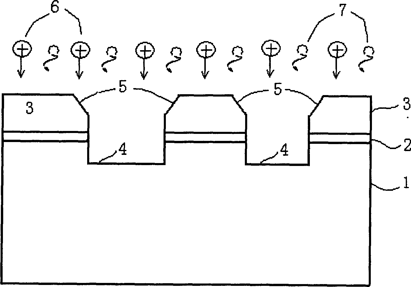
[0050]1. Deposit a layer of metal film on the sample with the lower cladding and core layer of the silica waveguide deposited in sequence. The thickness of the metal film is 1500 angstroms; the metal film is a composite metal film formed by a combination of Cr, Al, Au and Ni.
[0051] 2. Carry out a standard photolithography process on the metal film, and copy the waveguide pattern on the mask plate to the photoresist;
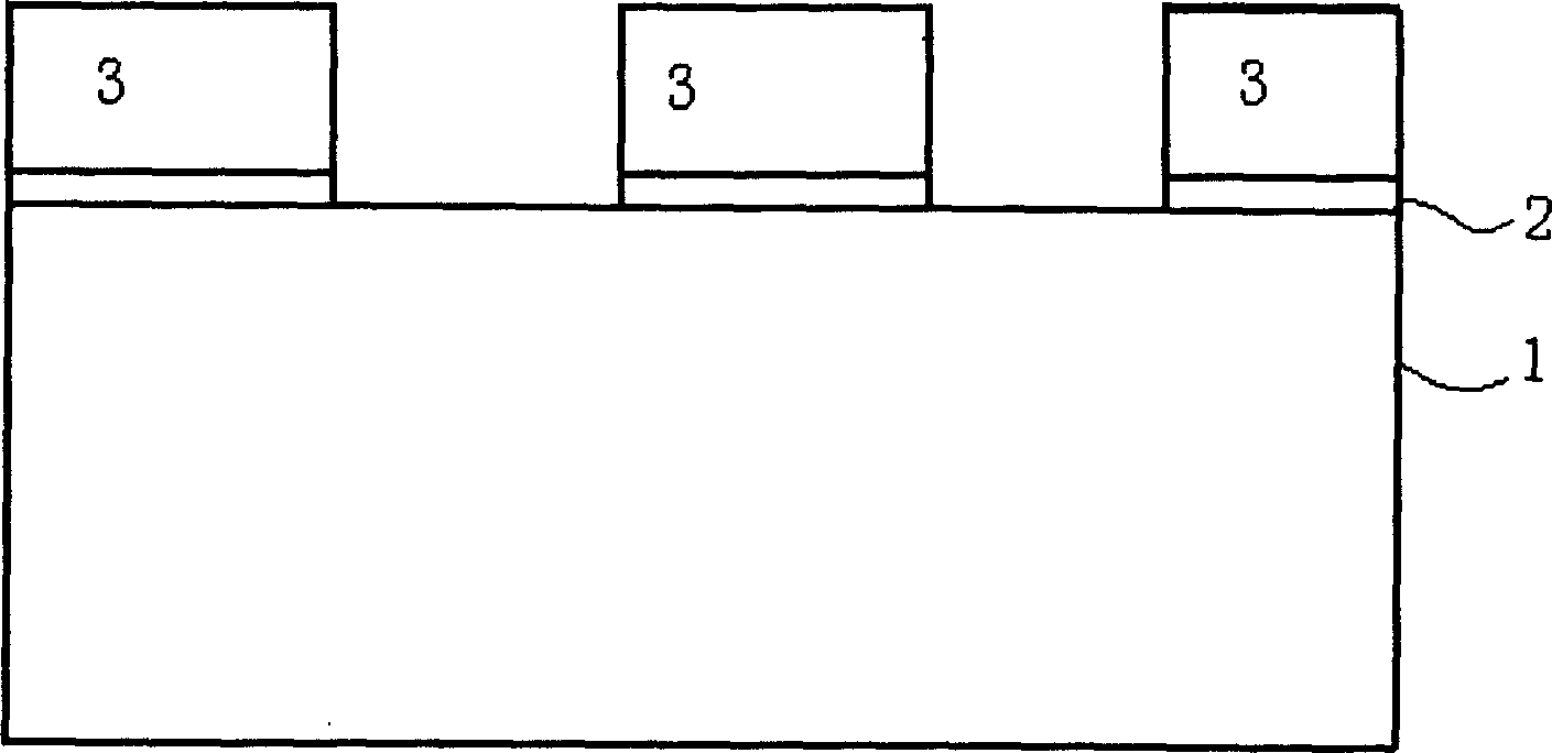
[0052] 3. Etching the metal film, the etching method can be chemical etching, or plasma etching, such as Cl 2 / O 2 , BCl 3 / O 2 plasma system, figure 1 It is a schematic diagram of the composite mask structure obtained after etching the metal film. In the figure, 1 is the silicon dioxide waveguide core layer, 2 is the metal film layer, and 3 is the photoresist layer;
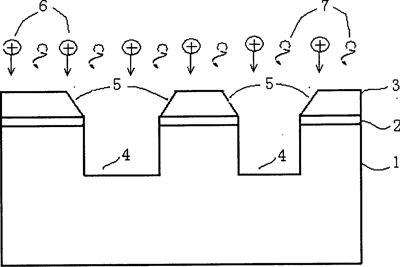
[0053] 4. Put the sample into the reactive ion et...
PUM
| Property | Measurement | Unit |
|---|---|---|
| thickness | aaaaa | aaaaa |
Abstract
Description
Claims
Application Information