Thin film transistor and producing method thereof

A technology of thin film transistors and manufacturing methods, which is applied in the direction of transistors, semiconductor/solid-state device manufacturing, electric solid-state devices, etc., can solve the problems of deterioration of working characteristics of thin-film transistors, and achieve the effect of excellent working characteristics and pollution suppression

Inactive Publication Date: 2005-02-09
MITSUBISHI ELECTRIC CORP
View PDF1 Cites 7 Cited by
  • Summary
  • Abstract
  • Description
  • Claims
  • Application Information

AI Technical Summary

Problems solved by technology

[0016] As mentioned above, in the conventional thin film transistor, in the manufacturing process up to the formation of the gate insulating film, since the natural oxide film is formed on the surface of the amorphous silicon film 10 and the polysilicon film 4, there is a problem that makes the operation of the thin film transistor difficult. The problem of deterioration of characteristics
In addition, in the photolithography process, there is a problem that the polysilicon film is not contaminated, which deteriorates the operating characteristics as a thin film transistor.

Method used


Image

  • Thin film transistor and producing method thereof
  • Thin film transistor and producing method thereof
  • Thin film transistor and producing method thereof

Examples


Embodiment approach 1

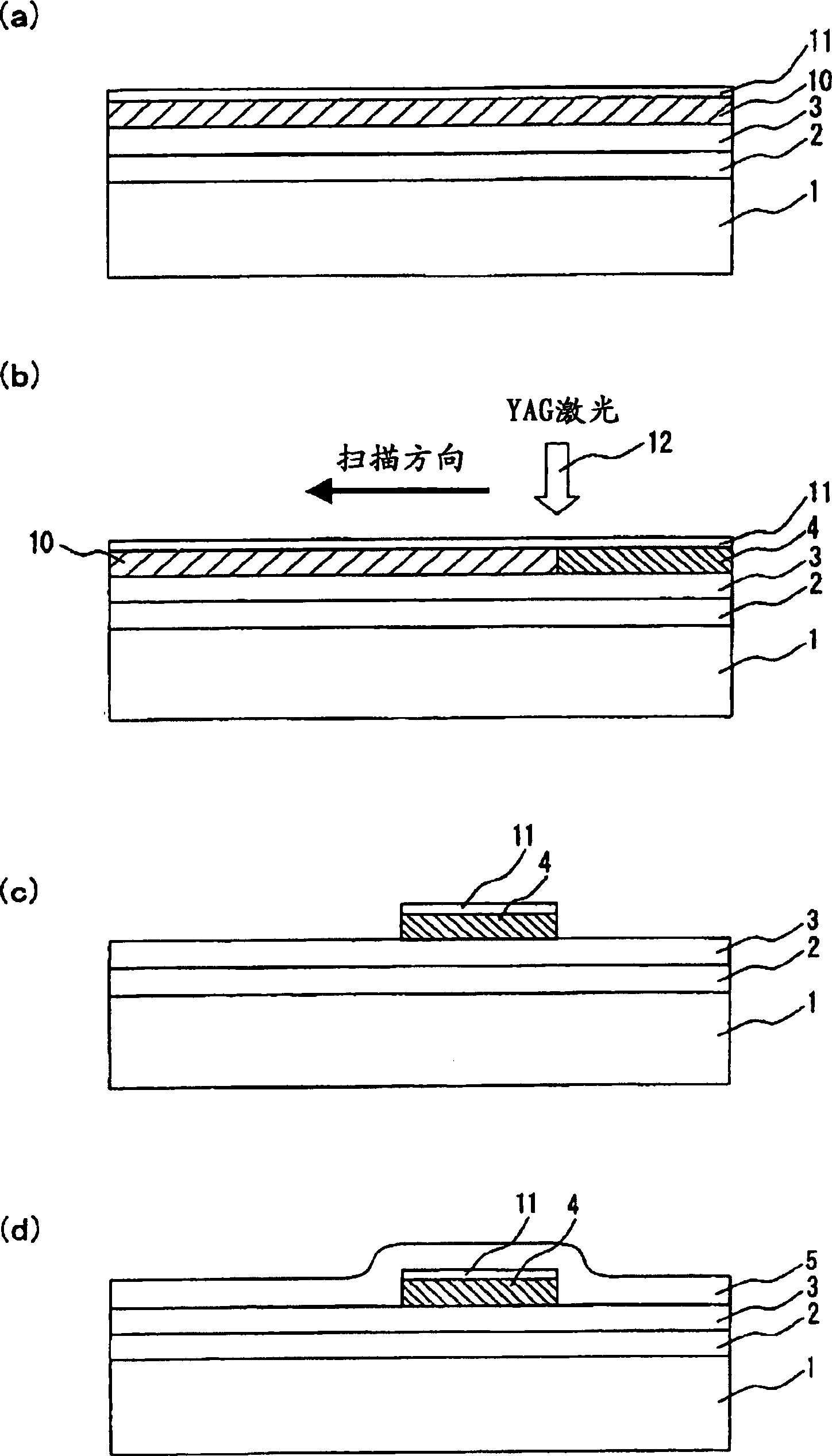
[0044] figure 1 (a)~ figure 1 (d) shows an example of the main part of the method for manufacturing a low-temperature polysilicon TFT according to Embodiment 1 of the present invention, and shows steps up to the formation of the gate insulating film 5 .

[0045] The insulating substrate 1 is an insulating transparent substrate such as a glass substrate, on which a silicon nitride film 2, a silicon oxide film 3, an amorphous silicon film 10, and a silicon oxide film 11 are sequentially formed. ( figure 1 (a) process). The amorphous silicon film 10 is an amorphous silicon film that is polycrystallized by laser irradiation described later and becomes an active semiconductor layer by ion doping. Both the silicon nitride film 2 and the silicon oxide film 3 are insulating undercoat films for stabilizing the characteristics of the semiconductor layer. The silicon oxide film 11 is an insulating interface protection film that prevents the amorphous silicon film 10 from being exp...

Embodiment approach 2

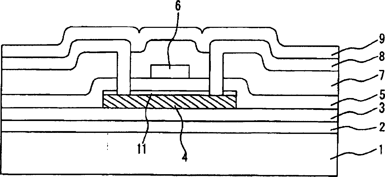
[0071] In Embodiment Mode 1, a method of manufacturing a thin film transistor in which the silicon oxide film 11 as an interface protective film is left is described. In this manufacturing method, until the silicon oxide film 5 serving as the gate insulating film is formed, it is considered that a native oxide film is formed on the surface of the silicon oxide film 11, and the defect level increases. Such a silicon oxide film 11 remains between the polysilicon film 4 and the gate electrode 6 of the thin film transistor. On the contrary, in this embodiment mode, by removing the silicon oxide film 11 after the photolithographic patterning, the operating characteristics as a thin film transistor are further improved.

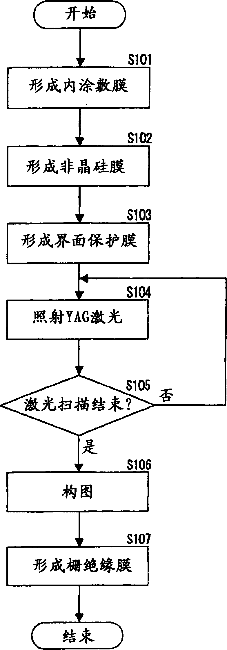
[0072] Figure 4 Steps S201 to S208 are a flowchart showing an example of main parts in the method of manufacturing a low-temperature polysilicon TFT according to Embodiment 2 of the present invention. From step S201 to step S206, and from image 3 The processin...

Embodiment approach 3

[0075] Figure 7 is a diagram showing an example of the main part of the method for manufacturing a low-temperature polysilicon TFT according to Embodiment 3 of the present invention, and figure 1 In the same manner as Embodiment 1 shown, each step up to the formation of the gate insulating film 5 is shown.

[0076] The insulating substrate 1 is an insulating transparent substrate such as a glass substrate, on which a silicon nitride film 2, a silicon oxide film 3, an amorphous silicon film 10, and a silicon oxide film 11 are sequentially formed. ( Figure 7 (a) process). The amorphous silicon film 10 is an amorphous silicon film that is polycrystallized by laser irradiation and becomes an active semiconductor layer by ion doping. Both the silicon nitride film 2 and the silicon oxide film 3 are insulating undercoat films for stabilizing the characteristics of the semiconductor layer. The silicon oxide film 11 is an insulating interface protection film that prevents the am...


PUM

PropertyMeasurementUnit
thicknessaaaaaaaaaa
thicknessaaaaaaaaaa
thicknessaaaaaaaaaa

Abstract

Provided is a manufacturing method of a thin film transistor extremely low in a defect level which is excellent in an operation property. The method includes steps of: forming an undercoat film comprising a silicon nitride film 2 and a silicon oxide film 3 on an insulating substrate 1; forming an amorphous silicon film 10 on the undercoat film; forming an interface protecting film comprising a silicon oxide film 11 on the silicon film 10; laser-annealing the silicon film 10 by irradiating a YAG laser on the substrate on which the interface protecting film is formed; patterning the silicon film 4 after laser annealing; and forming a gate insulating film comprising a silicon oxide film 5 on the substrate after patterning wherein the undercoat film, the amorphous silicon 10, and the interface protecting film are sequentially formed in a vacuum chamber while a vacuum state is maintained.

Description

technical field [0001] The present invention relates to a thin film transistor and a method of manufacturing the same, and more specifically, to a method of manufacturing a thin film transistor using polysilicon obtained by laser annealing amorphous silicon as a semiconductor layer, such as a thin film transistor constituting each pixel of a liquid crystal display device improvement of. Background technique [0002] A so-called active matrix liquid crystal display device is formed by forming a plurality of thin film transistors in a matrix on a glass substrate. Generally, an amorphous silicon film can be produced at a lower temperature than a silicon oxide film, so thin-film transistors using an amorphous silicon film as a semiconductor layer, so-called amorphous silicon TFTs, are widely used in conventional liquid crystal display devices. (Thin Film Transistor). [0003] However, thanks to the development of laser annealing technology for locally melting and crystallizing...

Claims


Application Information

Patent Timeline
Patent Type & Authority Applications(China)
IPC IPC(8): H01L21/20G02F1/136H01L21/02H01L21/336H01L29/786
CPCG02F1/136H01L27/124H01L29/66H01L29/786
Inventor 内田祐介寺元弘须贺原和之竹口徹
Owner MITSUBISHI ELECTRIC CORP
Why Eureka
Try Eureka