

Method for preparing single-layer capacitor element and its products
A capacitor and manufacturing method technology, applied in the direction of capacitor manufacturing, capacitors, electrical components, etc., can solve the problems of complex structure, complicated process, unreliable connection between electrodes, etc., and achieve good performance, low series equivalent resistance, and excellent performance. Effect
- Summary
- Abstract
- Description
- Claims
- Application Information
AI Technical Summary
Problems solved by technology
Method used
Image

Examples
Embodiment 1
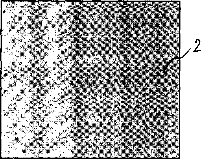
[0051] Such as figure 1 , 2The structure shown is one of the embodiments of the single-layer capacitor element of the present invention, which includes a 0.2mm thick single-layer ceramic dielectric layer 1 and an upper electrode layer 2 and a lower electrode layer respectively positioned on the opposite surfaces of the ceramic dielectric layer 1 3. The upper and lower electrode layers 2, 3 are firmly attached to the surface of the ceramic dielectric layer 1 through a vacuum high-energy sputtering process, and the upper and lower electrode layers 2, 3 are made of three layers of metal materials The metal material of the first layer is titanium, and the metal layer has the effect of enhancing the bonding force between the metal and the medium; the metal material of the second layer is nickel; the third layer, that is, the outermost metal material is gold; the upper and lower layers The electrode layers have the same or symmetrical metallization patterns; the upper and lower ele...
Embodiment 2
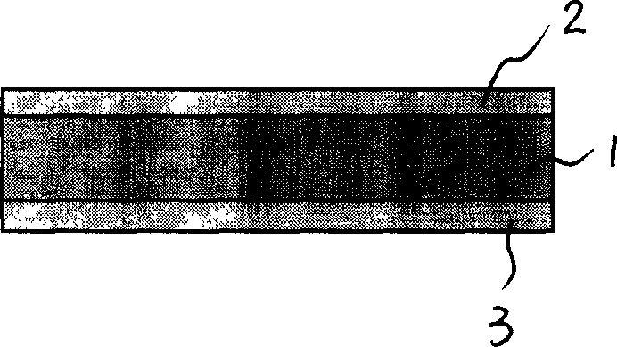
[0054] Such as image 3 , 4 The structure shown is the second embodiment of the single-layer capacitor element of the present invention, which includes a 0.125mm thick single-layer ceramic dielectric layer 1 and an upper electrode layer 2 and a lower electrode layer respectively positioned on the opposite surfaces of the ceramic dielectric layer 1 3. The upper and lower electrode layers 2, 3 are firmly attached to the surface of the ceramic dielectric layer 1 through a sputtering process, and the upper and lower electrode layers 2, 3 are composed of two layers of metal materials, Wherein the metal material of the first layer is titanium-tungsten alloy, and this metal layer has the function of strengthening the bonding force between metal and medium; the metal material of the second layer, the outermost layer, is gold-tin alloy; Or a symmetrical metallization pattern; there is a margin between the upper electrode layer and the surface of the ceramic dielectric layer to which i...
Embodiment 3
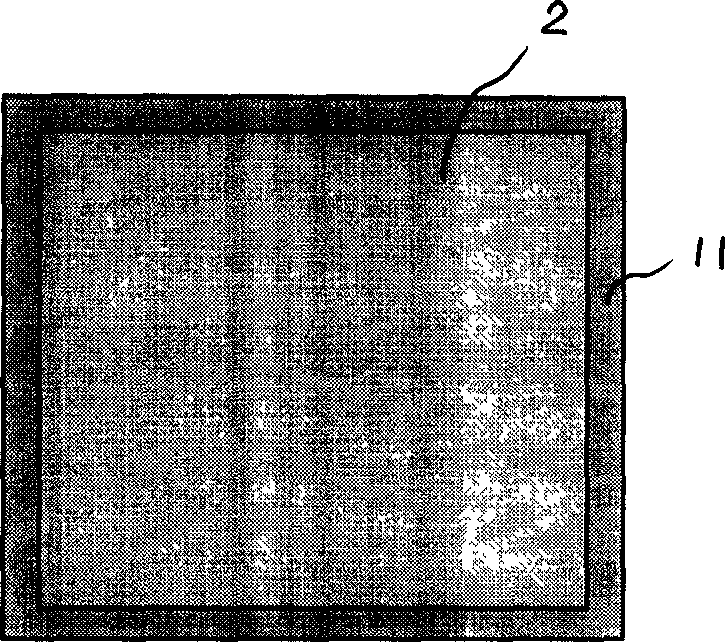
[0057] Such as Figure 5 , 6 The structure shown is the third embodiment of the present invention, which includes a 0.17mm thick single-layer ceramic dielectric layer 1 and an upper electrode layer 2 and a lower electrode layer 3 respectively located on two opposite surfaces of the ceramic dielectric layer 1. The upper and lower electrode layers 2, 3 are firmly attached to the surface of the ceramic dielectric layer 1 by a sputtering process, and the upper and lower electrode layers 2, 3 are composed of a layer of metal material, the metal material is gold ; There is the same or symmetrical metallization pattern between the upper and lower electrode layers; There is a margin 11 between the upper and lower electrode layers and the surface of the ceramic dielectric layer to which they are attached, and the upper margin and the surface of the ceramic dielectric layer The lower edge is symmetrical, this design is convenient for assembly, there is no distinction between upper and ...
PUM
| Property | Measurement | Unit |
|---|---|---|
| Capacitance | aaaaa | aaaaa |
| Resistance | aaaaa | aaaaa |
Abstract
Description
Claims
Application Information