Spring surface acoustic wave apparatus and communications equipment

A surface acoustic wave and filter technology, applied to electrical components, impedance networks, etc., can solve problems such as difficult to ensure heat dissipation routes, difficult heat dissipation measures, poor power resistance, etc.

Inactive Publication Date: 2006-01-04
KYOCERA CORP
View PDF0 Cites 11 Cited by
  • Summary
  • Abstract
  • Description
  • Claims
  • Application Information

AI Technical Summary

Problems solved by technology

[0011] However, if the CSP type is used, since the side of the piezoelectric substrate on which the IDT electrodes are formed is flip-chip-mounted toward the circuit substrate, it is difficult to implement a method for dissipating heat generated in the IDT electrodes due to high power loading. As a result of the previous heat dissipation measures, there is a problem that the power resistance is not good.
[0012] This is because, in the CSP type surface acoustic wave device, heat cannot be dissipated from the mounting surface side of the surface acoustic wave element of the piezoelectric substrate to the circuit substrate side only through conductor protrusions with a small cross-sectional area, and it is difficult to ensure an effective heat dissipation route.

Method used


Image

  • Spring surface acoustic wave apparatus and communications equipment
  • Spring surface acoustic wave apparatus and communications equipment
  • Spring surface acoustic wave apparatus and communications equipment

Examples


Embodiment 1

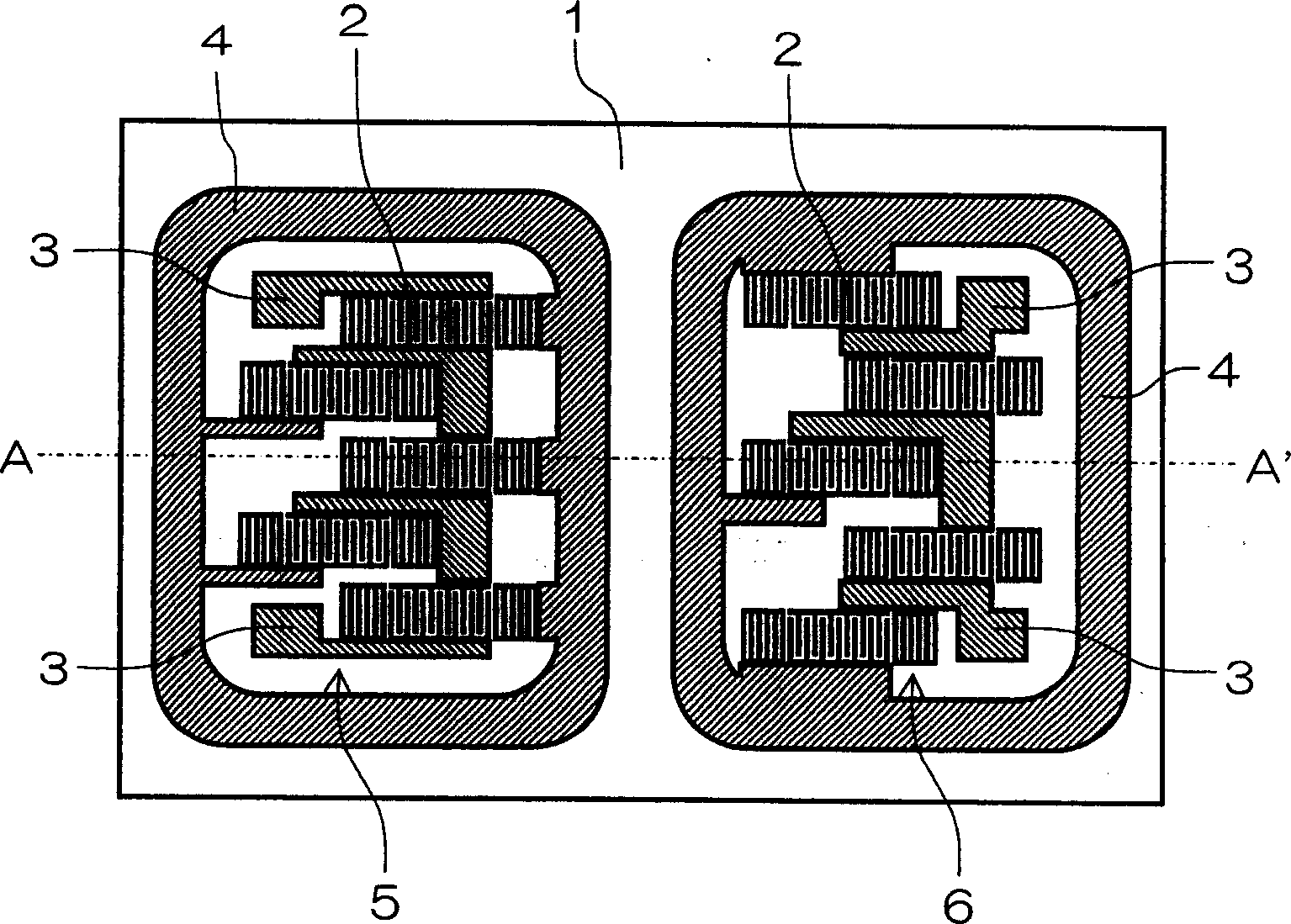
[0105] The piezoelectric substrate uses a lithium tantalate single crystal substrate that is transmitted in the 38.7°Y-tangential X direction. On one side of the main surface, an IDT made of an Al alloy of Al (99% by mass)-Cu (1% by mass) is formed. The pattern of the electrode 2, the pattern of the electrode pad as the input / output electrode, the pattern of the wiring electrically connecting them, and the ring electrode. These patterns are made as follows. After forming an Al alloy thin film by sputtering, photolithography is performed by a stepper exposure device, a spin coating device, and a developing device. After that, etching is performed by an RIE (reactive ion etching) device. In this way, given individual pattern formations are performed.

[0106] First, the lithium tantalate wafer serving as the piezoelectric substrate is ultrasonically cleaned with an organic solvent such as acetone or IPA (isopropyl alcohol), to clean the organic components. Next, after the subst...

Embodiment 2

[0118] Next, compare Figure 10 Another embodiment of the present invention will be described.

[0119] The piezoelectric substrate 1 uses a lithium tantalate single crystal substrate with a 36° Y-cut X transmission direction, and its chip size is 1.1 mm×1.5 mm. On the piezoelectric substrate 1, an IDT electrode 2, an input / output pad electrode 3, a ground pad electrode 4, a reflector 9, and a lead electrode 10 made of an Al-Cu alloy with a thickness of 1800 Å are formed by sputtering. The connecting wire 16 and the ring electrode 4 are photoresisted by a component device, a spin coating device, a developing device, etc., and then etched by a RIE (reactive ion etching) device to form a given pattern.

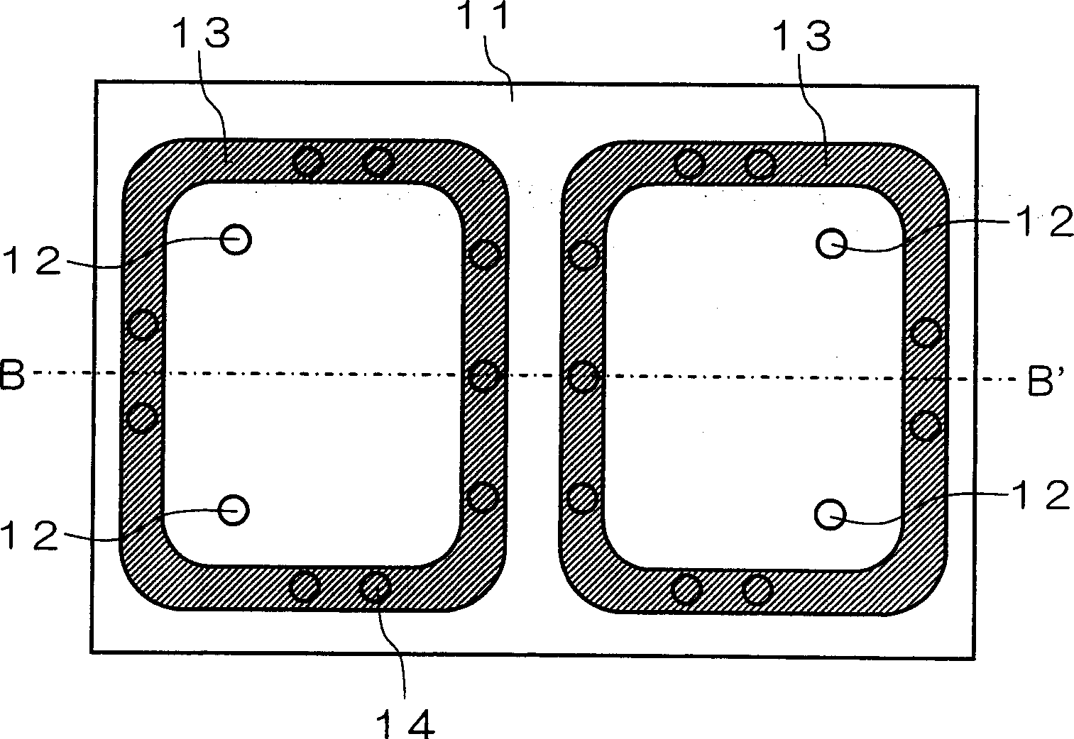
[0120] As the circuit board 11 , an LTCC (Low Temperature Co-fired Ceramics: Low Temperature Co-fired Ceramics) substrate with a substrate size of 70 mm×70 mm and a thickness of 250 μm was used.

[0121] On circuit board 11 , penetrating conductor 12 and sealing ring conductor...


PUM


Abstract

An IDT electrode (2) and an electrode pad (3) are formed at a primary face at one side of a piezoelectricity base plate (1), and an annular electrode (4) surrounding the IDT electrode (2) and the electrode pad (3) is formed. The annular electrode (4) is connected with a heat dissipation conductor (15) formed under a circuit base plate (11) through a through conductor (14) formed inside the circuit base plate (11), thus, heat produced by the IDT electrode (2) can be easily released to the outside by the annular electrode (4), the through conductor (14) and the heat dissipation conductor (15), which inhibits the bad influence caused by the heat and accordingly can improve the power withstanding performance of an elastic surface wave device.

Description

technical field [0001] The present invention relates to a surface acoustic wave (Surface Acoustic Wave, hereinafter abbreviated as SAW) device, in particular to a transmission and reception frequency divider (duplexer) used in communication devices that require small size and high power resistance. Surface acoustic wave device. Background technique [0002] In recent years, surface acoustic wave filters have been widely used in various communication devices. [0003] Surface acoustic wave filters have advantages such as steep filter characteristics and excellent mass production, so they are particularly suitable for mobile communication devices. [0004] In particular, a surface acoustic wave filter is also used as a filter constituting a duplexer inside a mobile communication device instead of a dielectric filter that has been used until now. [0005] However, the signal amplified by the power amplifier passes through the duplexer, so a high power of 0.8 to 1.2W is applie...

Claims


Application Information

Patent Timeline
Patent Type & Authority Applications(China)
IPC IPC(8): H03H9/25
Inventor 古贺亘生田贵纪船见雅之饭冈淳弘
Owner KYOCERA CORP
Why Eureka
Try Eureka