
Amorphous silicon film transistor with double grid structure and mfg. method thereof

A technology of an amorphous silicon thin film and a manufacturing method, which is applied in the directions of transistors, semiconductor/solid-state device manufacturing, semiconductor devices, etc., can solve the problems of reducing the reliability of amorphous silicon thin film transistors 1, insufficient current conduction capability, large operating voltage, etc.

Active Publication Date: 2006-01-11
AU OPTRONICS CORP
View PDF0 Cites 4 Cited by
  • Summary
  • Abstract
  • Description
  • Claims
  • Application Information

AI Technical Summary

Problems solved by technology

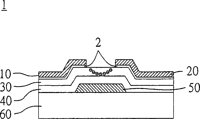
[0006] However, the current conduction capability of the conventional amorphous silicon thin film transistor 1 is insufficient, and the electron mobility (mobility) of its amorphous silicon channel layer 30 is usually less than 1 cm 2 / V-sec
To apply the amorphous silicon thin film transistor 1 to an active matrix organic light emitting diode (AMOLED) display, compared with the application of a polysilicon thin film transistor (poly-Si TFT) to an AMOLED A larger operating voltage is also required, and it will reduce the reliability of the amorphous silicon thin film transistor 1

Method used


Image

  • Amorphous silicon film transistor with double grid structure and mfg. method thereof
  • Amorphous silicon film transistor with double grid structure and mfg. method thereof
  • Amorphous silicon film transistor with double grid structure and mfg. method thereof

Examples


Embodiment 1

[0035] Please refer to Figure 2A-2F , which shows a process cross-sectional view of an amorphous silicon thin film transistor with a double-gate structure according to Embodiment 1 of the present invention. First, in Figure 2A Among them, a substrate 160 is provided, and a first gate 250 is formed on the substrate 160 . Wherein, the substrate 160 includes a glass substrate, a plastic substrate or an insulating substrate, and the first gate 250 includes a metal or a metal alloy.

[0036] Next, if Figure 2B As shown, a first insulating layer 240 is formed on the substrate 160 and covers the first gate 250 . Wherein, the first insulating layer 240 includes silicon nitride (silicon nitride, SiN), silicon oxynitride (silicon oxynitride, SiON), nitride, oxynitride or oxide.

[0037] Then, if Figure 2C As shown, an amorphous silicon channel layer 130 is formed on the first insulating layer 240 . Wherein, the amorphous silicon channel layer 130 is formed corresponding to the...

Embodiment 2

[0045] Please refer to Figures 3A-3H , which shows a process cross-sectional view of a thin film transistor with a double-gate structure according to Embodiment 2 of the present invention. First, if Figure 3A As shown, a substrate 360 ​​is provided, and a first gate 350 is formed on the substrate 360 ​​. Wherein, the substrate 360 ​​includes a glass substrate, a plastic substrate or an insulating substrate, and the first gate 350 includes a metal or a metal alloy.

[0046] Next, if Figure 3B As shown, a first insulating layer 340 is formed on the substrate 360 ​​and covers the first gate 350 . Wherein, the first insulating layer 340 includes silicon nitride, silicon oxynitride, nitride, oxynitride or oxide.

[0047] Then, if Figure 3C As shown, an amorphous silicon layer 330 is formed on the first insulating layer 340 .

[0048] Next, if Figure 3D As shown, an etch-stop layer 380 is formed on a portion of the amorphous silicon layer 330 , and the etch-stop layer 38...


PUM


Abstract

A non-crystalline silicon film transistor with double-grid structure includes a base plate, a first grid, a non-crystalline channel layer, a source a drain and a second grid. The first grid is formed on the base plate, the non-crystalline channel layer is formed on the first grid, the source and drain are formed on the channel layer corresponding to both ends of the first grid and contacted with both ends of the channel layer, the second grid is formed on the source and drain corresponding to the first grid and electrically connected with the first grid, edges of the second grid is overlapped with part of that of the source and drain and the non-crystalline channel is in the first grid.

Description

technical field [0001] The invention relates to a thin film transistor and a manufacturing method thereof, in particular to an amorphous silicon thin film transistor with a double gate structure and a manufacturing method thereof. Background technique [0002] Please refer to figure 1 , which shows a cross-sectional view of a conventional amorphous silicon thin film transistor (a-Si TFT). exist figure 1 Among them, the amorphous silicon thin film transistor 1 is basically an electronic element composed of a gate 50, a source 10, a drain 20 and an amorphous silicon channel layer 30, the gate 50 and the amorphous silicon channel layer 30 They are separated by an insulating layer 40 . The source 10 and the drain 20 are not in contact with each other, but are respectively in contact with the amorphous silicon channel layer 30 through the heavily doped N-type (N+) semiconductor layer 2 . [0003] When a voltage is applied to the gate 50 , the amorphous silicon channel layer 3...

Claims


Application Information

Patent Timeline
Patent Type & Authority Applications(China)
IPC IPC(8): H01L29/786H01L29/40H01L21/336H01L21/28
Inventor 陈纪文梁中瑜彭仁杰吴元均
Owner AU OPTRONICS CORP
Learn More