Semiconductor device and manufacturing method thereof

A manufacturing method and semiconductor technology, applied in the direction of semiconductor/solid-state device manufacturing, semiconductor devices, semiconductor/solid-state device components, etc., can solve problems such as process growth and achieve the effects of suppressing chip area, suppressing increase, and high sheet resistance

Inactive Publication Date: 2006-01-18
SANYO ELECTRIC CO LTD
View PDF1 Cites 3 Cited by
  • Summary
  • Abstract
  • Description
  • Claims
  • Application Information

AI Technical Summary

Problems solved by technology

These need to be carried out separately from the HEMT manufacturing process, and i

Method used


Image

  • Semiconductor device and manufacturing method thereof
  • Semiconductor device and manufacturing method thereof
  • Semiconductor device and manufacturing method thereof

Examples


Embodiment Construction

[0103] Embodiments of the present invention will be described in detail below.

[0104] First, refer to figure 1 and figure 2 A first embodiment of the present invention will be described.

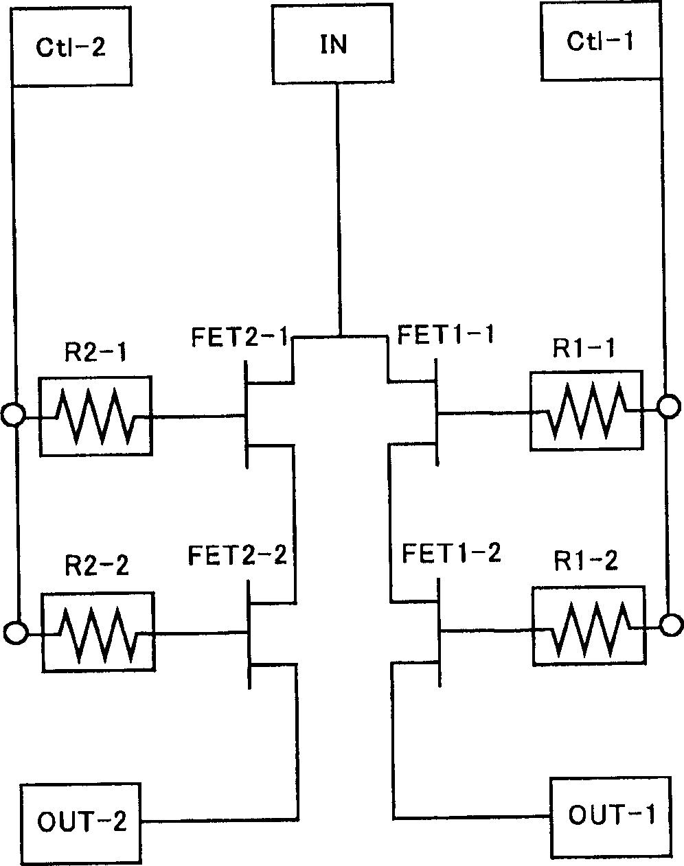
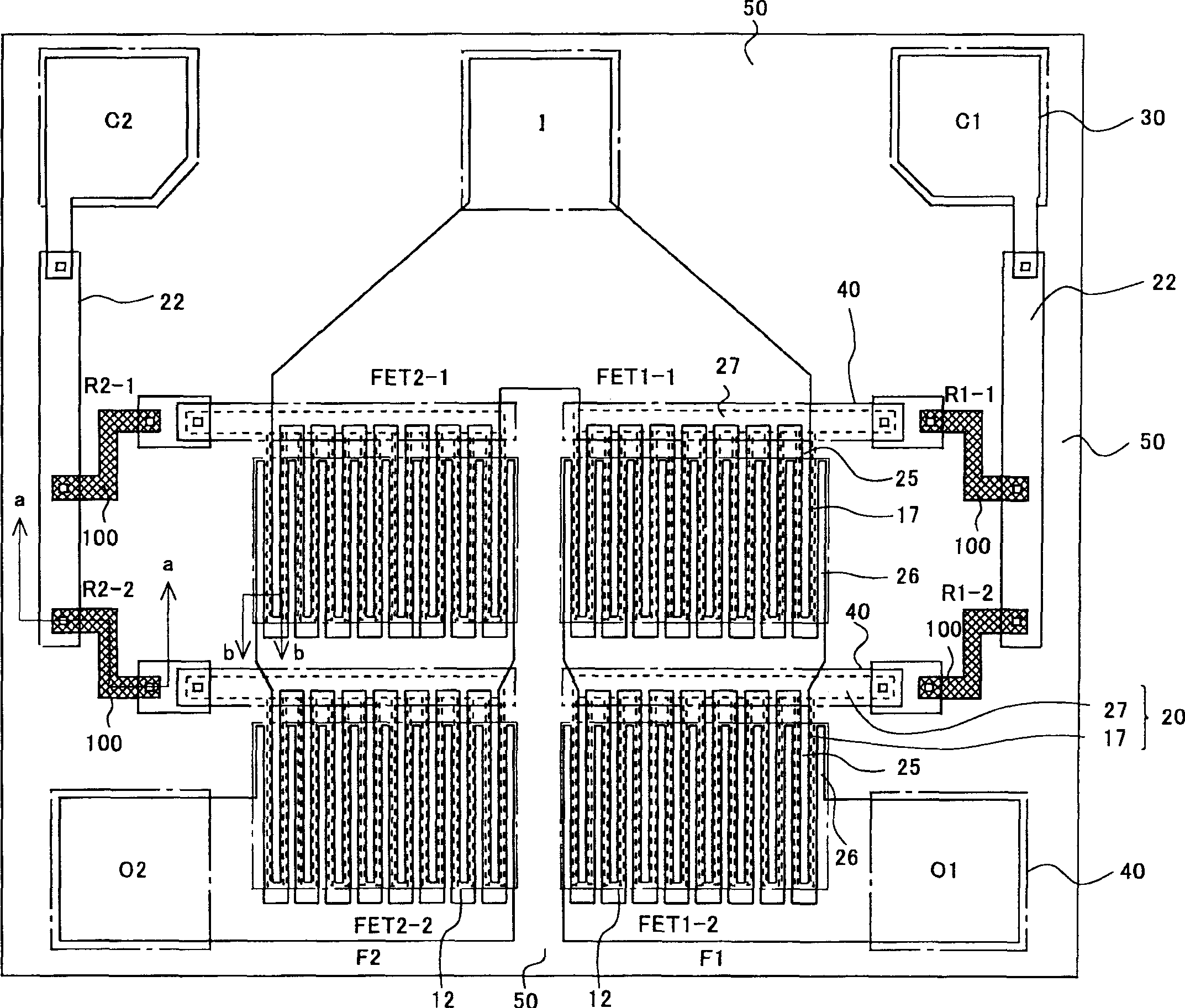
[0105] figure 1 is a diagram showing a semiconductor device in which HEMTs and resistor elements are monolithically integrated. Here, a switching circuit device called SPDT (Single Pole Double Throw) is shown, and a device in which HEMTs (FETs) are connected in series in multiple stages for high-power applications will be described as an example.

[0106] The control signals applied to the first and second control terminals Ctl-1 and Ctl-2 are complementary signals, which turn on the FET group on the side to which the H level signal is applied, and transfer the input signal applied to the common input terminal IN to any output terminal. Resistors are provided to prevent leakage of high-frequency signals from the DC potentials of the control terminals Ctl-1 and Ctl-2 connected to th...


PUM


Abstract

In the case where a HEMT and a resistor element are monolithically integrated, the resistor element has a low sheet resistance value since the resistor element includes a cap layer. If a resistor having a high resistance value is formed, it is required to extend the resistor for a long distance within a chip. As a result, a chip area is increased. A recessed part is provided by removing a cap layer in a predetermined shape, and resistor element electrodes are connected to both ends of the recessed part. A resistor layer is only a channel layer, and a sheet resistance value is high. Thus, a high resistance value can be obtained with a short distance. Since a sufficiently high resistance value can be obtained without extending a resistor for a long distance within a chip, a chip size can be reduced.

Description

technical field [0001] The present invention relates to a semiconductor device and a method of manufacturing the same, and more particularly, to a semiconductor device and a method of manufacturing the same that suppress an increase in the area occupied by a chip. Background technique [0002] In recent years, in mobile communication systems such as mobile phones, there has been a strong demand for miniaturization and low power consumption of terminal equipment. Therefore, miniaturization and low power consumption are also strongly demanded for various monolithic microwave integrated circuits (MMICs) used in RF (high frequency) circuits of transmission and reception systems. [0003] Among them, devices with heterojunction represented by HEMT (High Electron Mobility Transistor: High Electron Mobility Transistor) are compared with GaAs MESFET (Metal SemiconductorFET) and GaAs JFET (Junction FET) in terms of efficiency, gain, and distortion characteristics. Excellent, therefo...

Claims


Application Information

Patent Timeline
IPC IPC(8): H01L27/04H01L29/772H01L21/8234H01L21/336H03K17/687H01L21/20H01L21/338H01L21/822H01L23/522H01L23/544H01L23/62H01L27/06H01L27/095H01L29/778H01L29/812
CPCH01L2924/0002H01L23/62H01L2223/54453H01L23/544H01L23/5228H01L24/06H01L27/0605H01L2924/13062H01L2924/12032H01L2924/13063H01L2924/14H01L27/0629H01L2924/00H01L21/18H01L29/778
Inventor 浅野哲郎
Owner SANYO ELECTRIC CO LTD
Why Eureka
Try Eureka