Epitaxial growing technology of III class nitride semiconductor on silicon substrate

A nitride semiconductor and epitaxial growth technology, which is applied in the manufacture of semiconductor devices, semiconductor lasers, semiconductor/solid-state devices, etc., can solve problems such as high defect density and cracks in thick epitaxial layers, and achieve low dislocation density and easy operation. Effect of controlling and improving luminous efficiency

Inactive Publication Date: 2006-01-25
SHENZHEN UNIV
View PDF0 Cites 13 Cited by
  • Summary
  • Abstract
  • Description
  • Claims
  • Application Information

AI Technical Summary

Problems solved by technology

[0006] In the research process of silicon-based group III nitride epitaxy, various materials have been tried to be used as buffer layers to improve crystal quality, such as GaN grown at low temperature, AlN, AlAs, Si grown at low temperature and high temperature 3 N 4 , GaAs, ZnO, LiGaO 2 etc., but the defect density in crystal materials is too high, and the problem of cracks in thicker epitaxial layers is still the main obstacle restricting the development of silicon-based III-nitride materials and devices

Method used


Image

  • Epitaxial growing technology of III class nitride semiconductor on silicon substrate

Examples


Embodiment Construction

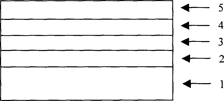
[0018] 1. Use the following cleaning solution H for the single-sided or double-sided polished silicon wafer 2 SO 4 :H 2 o 2 , NH 4 OH:H 2 o 2 :H 2 O, HCl:H 2 o 2 :H 2 O, HF:H 2 O and rinse with copious amounts of cold and hot deionized water; spin dry.

[0019] 2. Put the cleaned and dried silicon wafer into the PECVD reaction chamber to deposit SiO 2 ; Or put it into an oxidation furnace to oxidize to the required thickness of the oxide layer.

[0020] 3. Deposit SiO 2 Or put the oxidized silicon wafer into the MOCVD reaction chamber immediately after taking it out.

[0021] 4. Rapidly raise the temperature of MOCVD to 1000°C ~ 1150°C, while passing H 2 .

[0022] 5. Grow the buffer layer 3AlN, the growth time is 200 seconds to 450 seconds, and pass NH at the same time 3 and trimethylaluminum (TMAl).

[0023] 6. Grow the gradient layer 4 rich in Ga-GaN, the growth time is about 200 seconds to 800 seconds, pass NH 3 and trimethylgallium (TMG); the flux of tri...


PUM

PropertyMeasurementUnit
Thicknessaaaaaaaaaa

Abstract

This invention relates to a new technology for growing group III nitride semiconductor mono-crystal material, which grows two buffer layer and one graded bedding before growing the semiconductor material, buffer layer 2 is SiO2 film, buffer layer 3 is AIN film and the graded bedding is a rich GaN grown under high temperature and deviating from the chemical test ratio. The two buffer layers and the graded bedding structure can reduce the crack of nitride group III semiconductor mono-crystal material due to the too large difference of the thermal expansion factor between the substrate and the material and the high defect concentration because of the mismatched lattices.

Description

1. Technical field [0001] The invention relates to a method for obtaining high-quality heteroepitaxial Group III nitride crystal material by using double buffer layer plus gradient layer technology. 2. Technical background [0002] Group III nitride semiconductors have been widely used in light-emitting diodes, semiconductor lasers and other high-performance electronic devices due to their excellent optoelectronic properties. [0003] Due to the lack of GaN base single crystals, GaN-based optoelectronic devices are currently epitaxy through heterogeneous substrates. At present, the heterogeneous substrates used in commercial production mainly include Al 2 o 3 and SiC, although Al 2 o 3 The process of epitaxial growth of GaN on SiC and SiC single crystal is relatively mature, and GaN-based light-emitting diodes and semiconductor lasers have been introduced; but the price of SiC is expensive, which seriously restricts the popularization and application of corresponding dev...

Claims


Application Information

Patent Timeline
IPC IPC(8): H01L21/20H01L21/316H01L33/00H01S5/00H01L33/32
Inventor 冯玉春郭宝平牛憨笨李忠辉
Owner SHENZHEN UNIV
Why Eureka
Try Eureka