Semiconductor device and method of fabricating the same

A manufacturing method, semiconductor technology, applied in semiconductor/solid-state device manufacturing, semiconductor devices, semiconductor/solid-state device components, etc., can solve problems such as damaging the surface of semiconductor layers, increasing the process of removing polymers, and uneven contact resistance

Active Publication Date: 2006-01-25
SAMSUNG DISPLAY CO LTD
View PDF1 Cites 14 Cited by
  • Summary
  • Abstract
  • Description
  • Claims
  • Application Information

AI Technical Summary

Problems solved by technology

[0008] However, in the above method of forming a contact hole, as figure 2 As shown, dry etching will form a polymer 21 under the contact hole 18, the contact hole 18 has penetrated the interlayer dielectric 17 and the gate insulating layer 14 and exposed the surface of the semicondu

Method used


Image

  • Semiconductor device and method of fabricating the same
  • Semiconductor device and method of fabricating the same
  • Semiconductor device and method of fabricating the same

Examples


no. 1 example

[0035] Figures 3A-3E is a cross-sectional view showing a method of forming a contact hole according to an embodiment of the present invention and a process of using the contact hole.

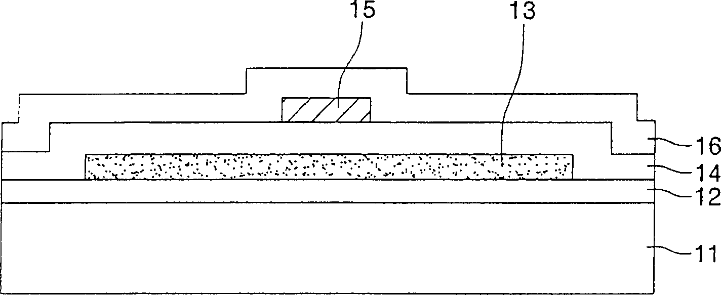
[0036] first, Figure 3A It is a cross-sectional view of the process of forming a buffer layer, a semiconductor layer, a gate insulating layer, a gate electrode and an interlayer dielectric on a substrate. Such as Figure 3A As shown, a buffer layer 102 is formed on an insulating substrate 101 such as plastic or glass. The buffer layer 102 functions to prevent the diffusion of water vapor or impurities generated from the insulating substrate, or to facilitate the crystallization of the semiconductor layer by adjusting the heat conduction rate when crystallization is performed.

[0037] Next, an amorphous silicon layer is formed on the buffer layer 102 , and then the amorphous silicon layer is crystallized into a polycrystalline silicon layer or a single crystal silicon layer, which is patter...

no. 2 example

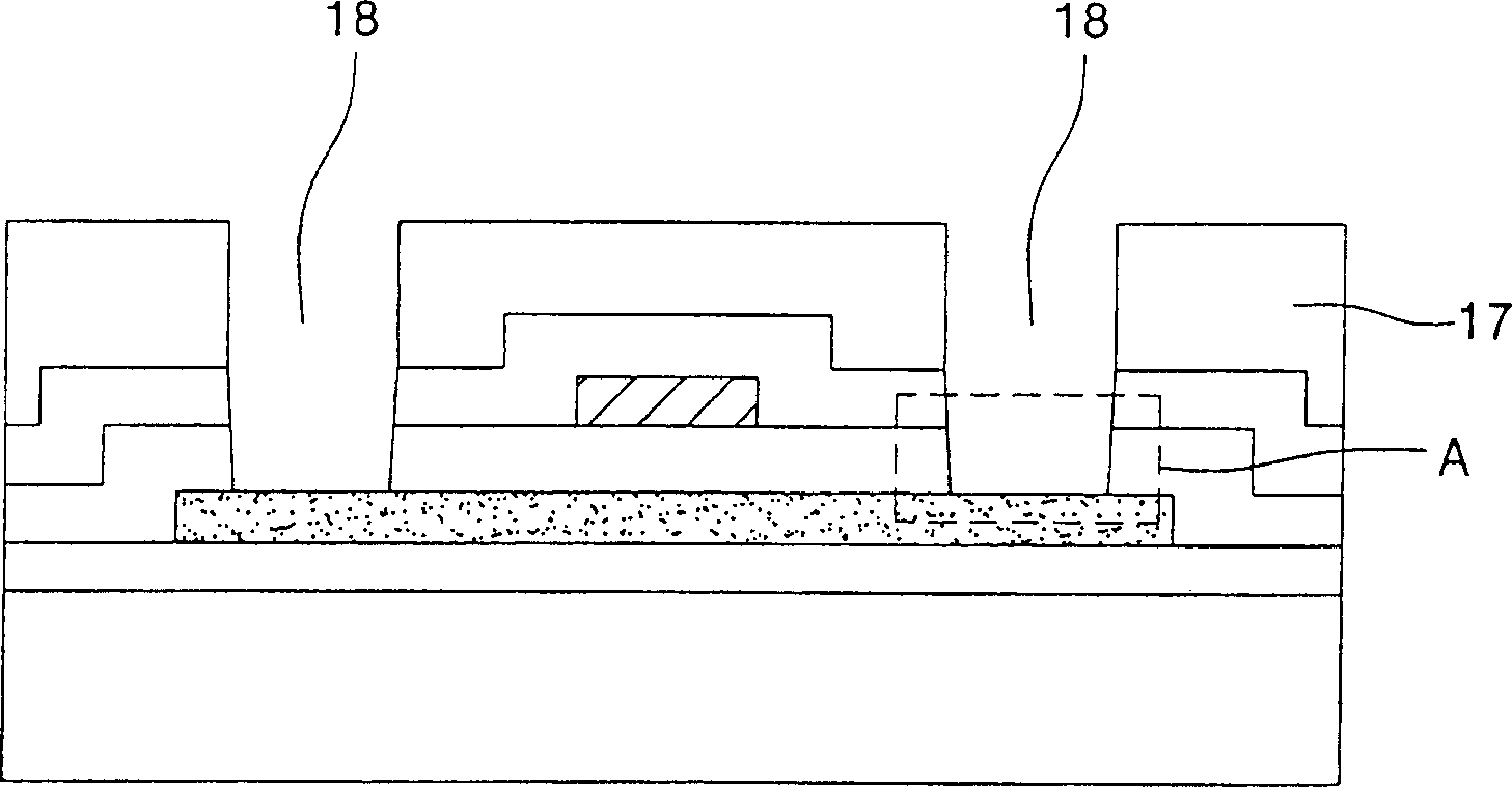
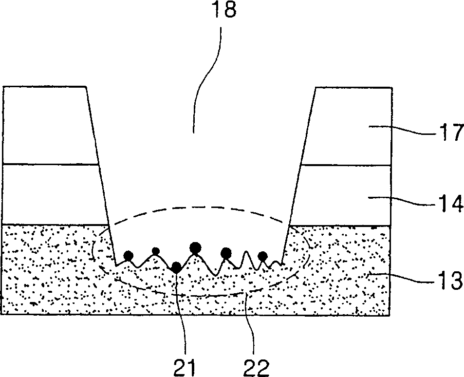
[0053] Figures 4A-4G are sectional views showing a method of forming a contact hole according to another embodiment of the present invention, and a sectional view and a sectional photograph of a process using the contact hole.

[0054] first, Figure 4A is a sectional view illustrating the steps of forming a buffer layer, a semiconductor layer, a gate insulating layer, a gate electrode, and an interlayer dielectric on a substrate. Such as Figure 4A As shown, a buffer layer 152 is formed on an insulating substrate 151 such as plastic or glass. The buffer layer 152 functions to prevent the diffusion of water vapor or impurities generated from the insulating substrate, or to facilitate the crystallization of the semiconductor layer by adjusting the heat conduction rate when crystallization is performed.

[0055] Next, an amorphous silicon layer is formed on the buffer layer 152 , and then the amorphous silicon layer is crystallized to form a polycrystalline silicon layer or ...

no. 3 example

[0081] Figures 5A-5E is a sectional view showing a method of forming a through hole and a process of using the through hole according to another embodiment of the present invention.

[0082] first, Figure 5A is a cross-sectional view of the steps of forming a buffer layer, a semiconductor layer, a gate insulating layer, a gate electrode, an interlayer dielectric, and source and drain electrodes on a substrate. Such as Figure 5A As shown, a buffer layer 202 is formed on an insulating substrate 201 such as plastic or glass.

[0083] Next, an amorphous silicon layer is formed on the buffer layer 202 , and then the amorphous silicon layer is crystallized into a polycrystalline silicon layer or a single crystal silicon layer and patterned to form the semiconductor layer 203 . In this case, a CVD method or a PVD method may be used for the amorphous silicon layer.

[0084] Next, a gate insulating layer 204 is formed over the entire surface of the substrate in which the semicon...


PUM

PropertyMeasurementUnit
Cone angleaaaaaaaaaa

Abstract

The present invention relates to a semiconductor device and a manufacturing method thereof. When a contact hole of a semiconductor layer and a source and drain electrode, a through-hole of a positive electrode and the source and drain electrode, a through-hole between connecting metal lines or a contact hole of the through-holes, are formed, at least one type of dry-process corrosion of high corrosion rate and high selectivity is used for dry-process corrosion; wet-process corrosion is adopted in the final corrosion treatment, so as to form the contact holes, the through-holes or the contact holes of the through-holes, which are provided with various conical angles and a plurality of contours; residues that are produced by corrosion can be completely eliminated in the wet-process and dry-process treatment; therefore, the contact holes, the through-holes or the contact holes of the through-holes have excellent contact characteristics. The semiconductor device comprises a substrate, a film transistor that is formed on the substrate and is provided with a semiconductor layer, a grid insulation layer, a grid electrode and a interlayer dielectric, and contact holes that penetrates the grid insulation layer and the interlayer dielectric, is exposed on the surface of the semiconductor layer and is provided with a plurality of contours. The upper part of the contact holes is provided with a contour for the wet-process corrosion; and the lower part has at least one of the contours for the wet-process corrosion and the dry-process corrosion.

Description

technical field [0001] The present invention relates to a semiconductor device and a manufacturing method thereof, more particularly, to a semiconductor device and a manufacturing method thereof, the manufacturing method comprising: when forming a semiconductor layer and contact holes for source and drain electrodes, a When using at least one of high etch rate dry etch and high selectivity dry etch during via holes, via holes between metal interconnect lines, or via contact holes, and in the final etch process Wet etching is carried out in the process, so that the contact hole, via hole or through-hole contact hole can be formed into various profiles with different cone angles, and the corrosion residue due to etching can be completely removed when wet-dry processing is performed , so that the contact hole, the through hole and the through hole contact hole can have excellent contact performance. Background technique [0002] Generally, silicon thin film transistors (TFTs) ...

Claims


Application Information

Patent Timeline
IPC IPC(8): H01L29/786H01L21/336H01L21/30H01L21/306H01L21/3065H01L21/768H01L21/8234H01L23/52H01L21/28H01L23/522H01L51/50H05B33/10H05B33/14H05B33/22H05B33/26
Inventor 姜泰旭郑仓龙金昌树徐昌秀朴汶熙
Owner SAMSUNG DISPLAY CO LTD
Why Eureka
Try Eureka