Method for bonding nanometer material on metal electrode

A technology of metal electrodes and nanomaterials, applied in the field of nanometers, can solve problems such as inability to simplify and batch, incompatibility with IC technology, and incompatibility with IC technology, and achieve low cost, firm and reliable contact, and simple equipment.

Inactive Publication Date: 2006-02-22
SHANGHAI JIAO TONG UNIV
View PDF0 Cites 52 Cited by
  • Summary
  • Abstract
  • Description
  • Claims
  • Application Information

AI Technical Summary

Problems solved by technology

In addition, in this paper, SEM is used to irradiate the place where the carbon tube contacts the metal electrode, the processing efficiency is low, and it is not compatible with the IC process
In short, the existing methods either require expensive equipment such as electron beam lithography when manufacturing contacts, or are incompatible with existing integrated circuit processes, and cannot be simplified and mass-produced

Method used


Image

  • Method for bonding nanometer material on metal electrode

Examples


Embodiment 1

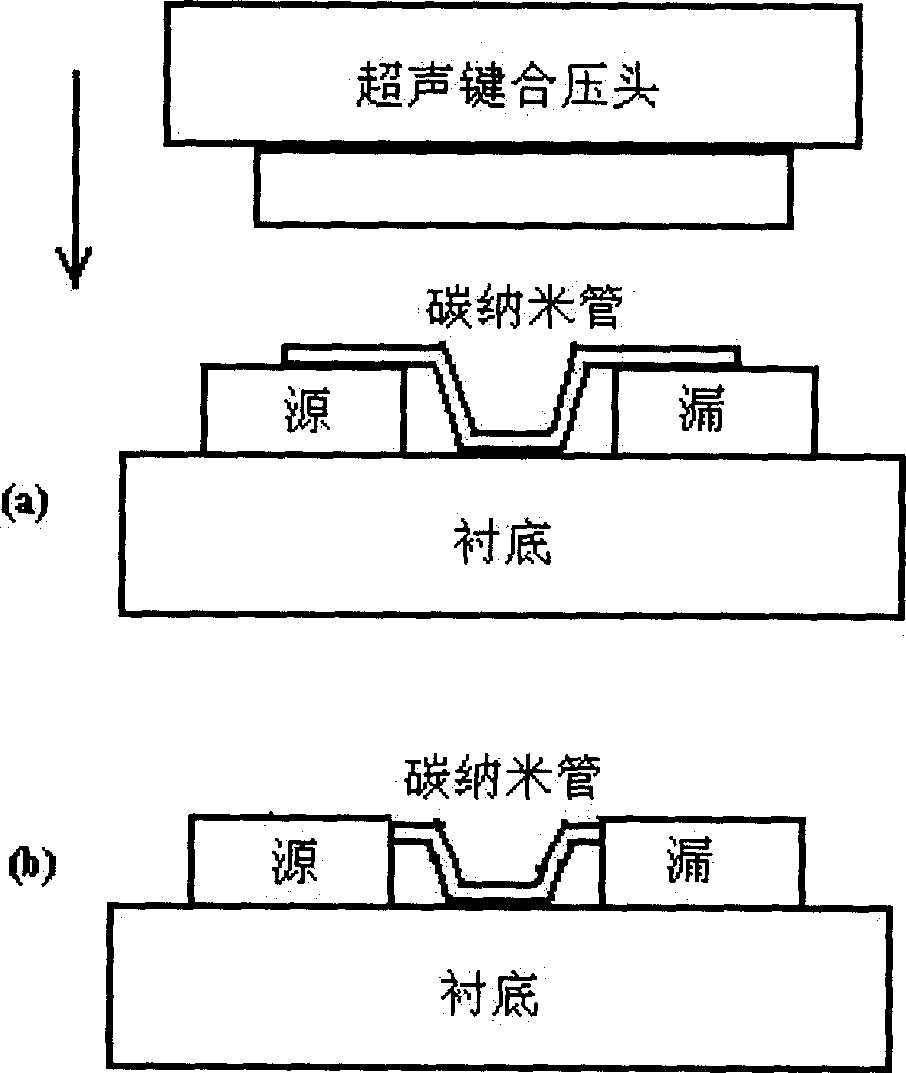
[0017] A single carbon nanotube bundle is connected between the Au electrodes on the chip, so that the end of the carbon nanotube rests on the surface of the electrode. Using a wire bonder, ultrasonically bond the contacts. The ultrasonic power is 10W, the ultrasonic time is 500ms, the extrusion pressure is 0.01N, the bonding head is preheated to 400 degrees, and the chip is preheated to 300 degrees. At the end, the carbon nanotubes are welded together with the metal electrodes. Before ultrasonic bonding, carbon nanotube bundles remain on the electrode surface, but after ultrasonic bonding, it can be found that carbon nanotubes and electrodes are welded together, almost no CNT can be seen on the electrode surface, and CNT is embedded in the electrode. Finally, the i-v curves before and after pressure welding were measured with a precision semiconductor parameter tester. The results showed that the two-terminal resistance dropped by 3-4 orders of magnitude, from 55MΩ before pr...

Embodiment 2

[0019] A single Si nanowire is connected between the Al electrodes on the chip, so that the end of the carbon nanotube rests on the upper surface of the electrode. The contacts are ultrasonically bonded using a wire bonder. The ultrasonic power is 30W, the ultrasonic time is 1ms, the extrusion pressure is 2.5N, the bonding head is not preheated, and the chip is not preheated. Since the bonding part of the bonding head covers the end of the carbon nanotube in contact with the electrode, the carbon nanotube The tubes are welded together with metal electrodes. The Si nanowires on the electrode after ultrasonic bonding and the electrode are welded together. The Si nanowires are almost invisible on the surface of the electrode. The Si nanowires are embedded in the electrode, forming a firm and reliable contact, and the two-terminal resistance is reduced by 3 -4 orders of magnitude.

Embodiment 3

[0021] A plurality of SiC nano whiskers are connected between the SiAl electrodes on the chip, so that the ends of the carbon nanotubes are pressed on the lower surface of the electrodes. The contacts are ultrasonically bonded using a wire bonder. The ultrasonic power is 0W, the ultrasonic time is 1000ms, the extrusion pressure is 1N, the bonding head is preheated to 200 degrees, and the chip is preheated to 150 degrees. After the SIC nano whiskers on the two electrodes are ultrasonically bonded, they form a firm and reliable contact with the electrodes, and the two-terminal resistance drops by 3-4 orders of magnitude.


PUM


Abstract

Disclosed a method for bonding nanometer material on the metal electrode, belongs to the nanometer technique filed. Wherein, connecting the one-dimensional nanometer material between the metal electrodes of chip, to make its end part on the face of metal electrode or under its low surface; using the ultrasonic wave header which carries ultrasonic wave to press and weld the one-dimensional nanometer material and the contact part of metal electrode as a whole. The invention reaches the reliable contact between the one-dimensional nanometer material and metal electrode to reduce the contact resistance significantly; since the device for ultrasonic welding belongs to the integrated circuit packaging processing, the one-dimensional nanometer material of a plurality of metal electrodes can be fast welded in batch; and has simple device and lower cost compared to other method which also can reduce the contact resistance.

Description

technical field [0001] The invention relates to a method in the field of nanotechnology, in particular to a method for bonding nanomaterials on metal electrodes. Background technique [0002] Due to their unique electrical and mechanical properties, nanomaterials have great application prospects in the production of functional materials and molecular devices. Among them, quasi-one-dimensional nanomaterials such as carbon nanotubes, silicon nanowires, silicon carbide nanowhiskers, oxide nanobelts, etc. can be used as metal electrode connections to achieve excellent functions, and can also be used as interconnecting wires for circuits. However, quasi-one-dimensional nanomaterials are difficult to form good electrical contact with metal electrodes when making devices or interconnections. The analysis shows that there are two main reasons for the high contact resistance between the quasi-one-dimensional nanomaterials and metal electrodes: (1) If the quasi-one-dimensional nanoma...

Claims


Application Information

Patent Timeline
Patent Type & Authority Applications(China)
IPC IPC(8): H01L21/607H01L21/28H01L21/768
Inventor 张亚非陈长鑫徐东
Owner SHANGHAI JIAO TONG UNIV
Why Eureka
Try Eureka