Quickflashing memory unit and its manufacturing method

A storage unit and manufacturing method technology, applied in semiconductor/solid-state device manufacturing, electrical components, electrical solid-state devices, etc., can solve problems such as high process difficulty, slow component operation speed, and increase the complexity of the back-end process, to achieve The effect of increasing the reading rate and improving the performance of the device

Inactive Publication Date: 2006-04-26
POWERCHIP SEMICON CORP
View PDF1 Cites 12 Cited by
  • Summary
  • Abstract
  • Description
  • Claims
  • Application Information

AI Technical Summary

Problems solved by technology

However, since the aspect ratio of the contact plug opening is very large, and two different materials need to be etched, it is difficult to control the depth of the contact plug opening, so the process difficulty is high
Moreover, in the back-end process, since the contact plugs in the memory cell area and the contact plugs in the peripheral circuit area must be formed separately, the complexity of the back-end process will also be increased.
[0004] In addition, due to the poor contact between the contact plug 60a and the drain region 44 and the shallow well region 46 (the contact window 60a and the drain region 44 are in vertical contact, and the contact area between the two is small), when operating this memory cell (especially When performing a read operation on the memory cell), the resistance value of the drain region 44 and the shallow well region 46 will become larger or unstable, resulting in a slower operating speed of the device, thereby affecting the performance of the device

Method used


Image

  • Quickflashing memory unit and its manufacturing method
  • Quickflashing memory unit and its manufacturing method
  • Quickflashing memory unit and its manufacturing method

Examples


no. 1 example

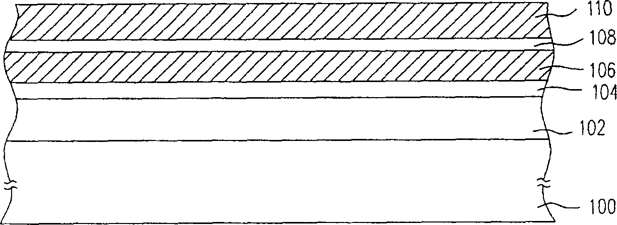
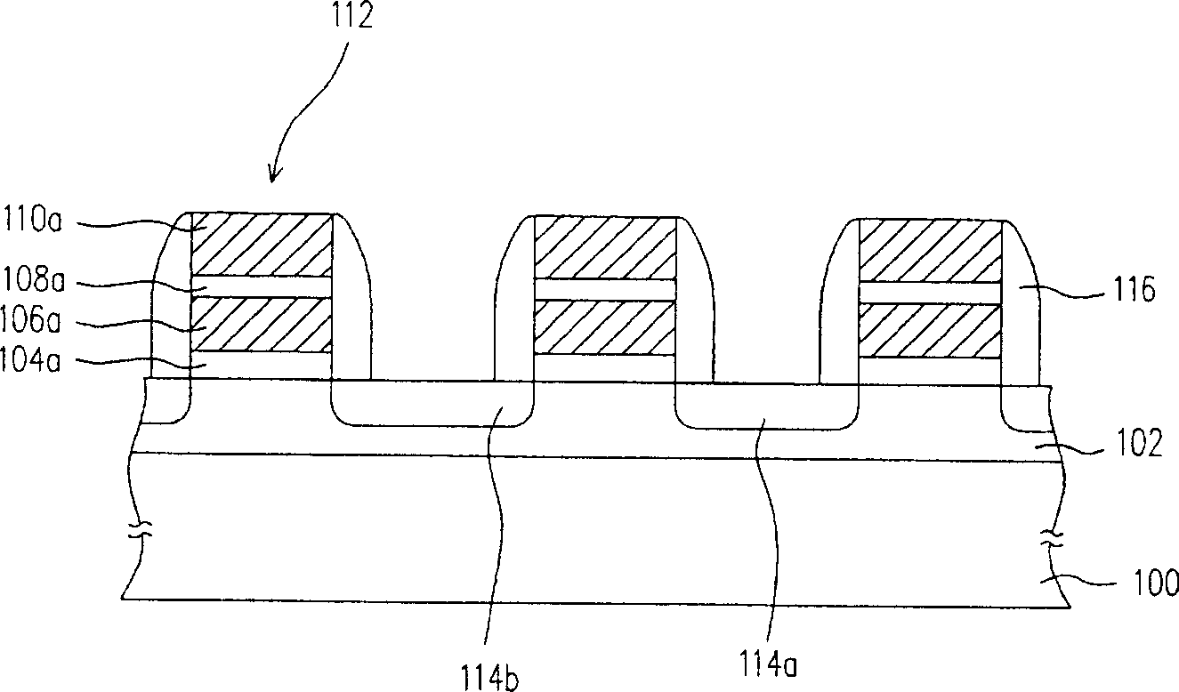
[0048] Figure 2A to Figure 2E A cross-sectional view of a manufacturing process of a flash memory unit according to a preferred embodiment of the present invention is shown.

[0049] Please refer to Figure 2A First, a p-type shallow well region 102 is formed in an n-type substrate 100 , and then a dielectric layer 104 , a conductive layer 106 , a dielectric layer 108 and a conductive layer 110 are sequentially formed on the n-type substrate 100 . Wherein, the material of the dielectric layer 104 is, for example, silicon oxide, and its forming method is, for example, thermal oxidation. The material of the dielectric layer 108 is, for example, silicon oxide / silicon nitride / silicon oxide, etc., or is composed of a silicon oxide layer or a silicon oxide / silicon nitride layer, etc., and its formation method is, for example, Low Pressure Chemical Vapor Deposition (Low Pressure CVD) , LPCVD). The material of the conductor layer 106 and the conductor layer 110 is, for example, po...

no. 2 example

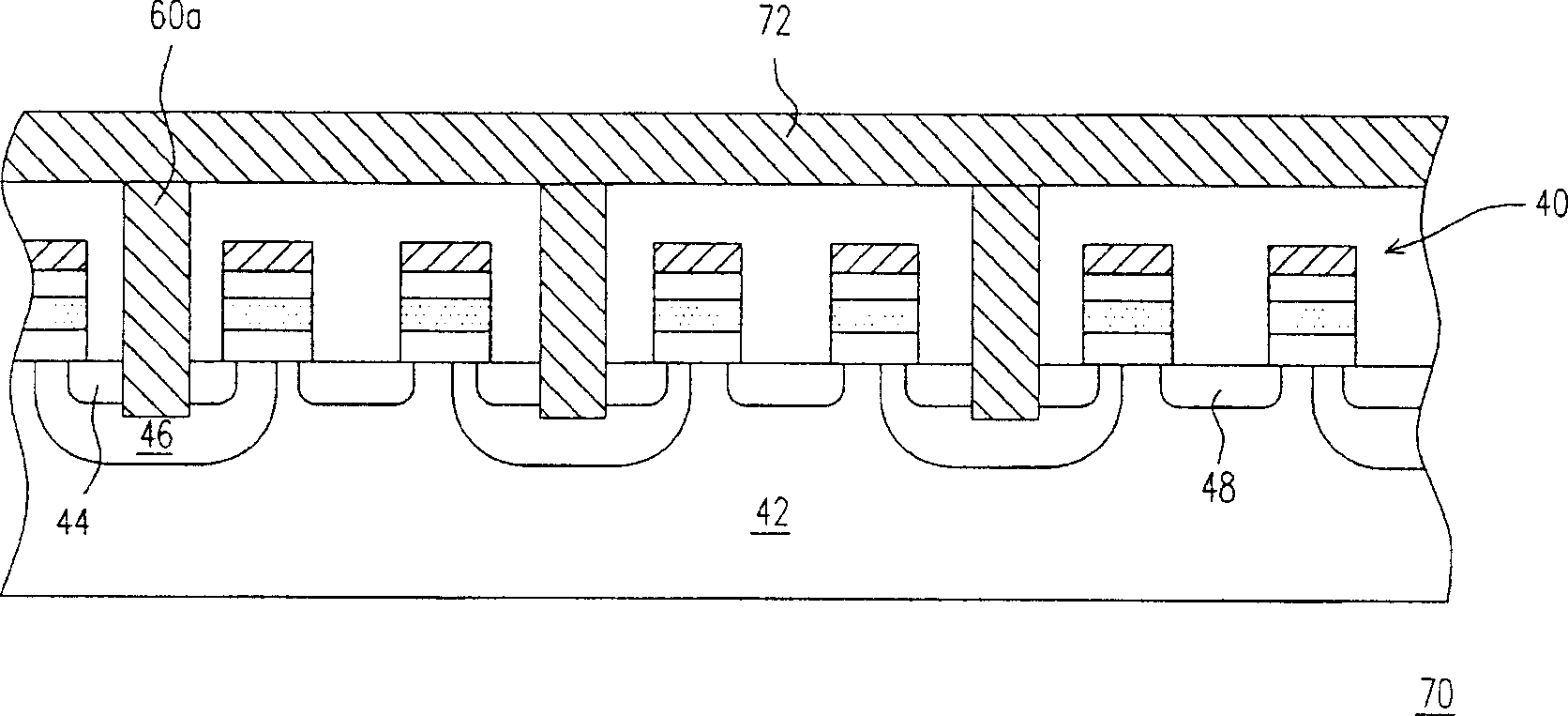
[0063] In the present invention, the doped region can also be formed in the n-type drain region and the p-type shallow well region first, and then a metal silicide layer is formed in the n-type drain region, so as to reduce the energy required in the process of forming the doped region . Figure 3A to Figure 3B That is a cross-sectional view of a part of the manufacturing process of a flash memory unit according to another preferred embodiment of the present invention. The components in this embodiment are the same as those in the first embodiment, that is, they are denoted by the same reference numerals. For the forming method and materials, please refer to the description of the first embodiment, and will not be repeated below.

[0064] Please refer to Figure 3A , according to the above example Figure 2A to Figure 2B completed by the description of Figure 2BAfter the structure shown, a photoresist layer 122 with an opening 124 is then formed on the n-type substrate 100...

no. 3 example

[0068] Figure 4A to Figure 4B A schematic cross-sectional view of a part of the manufacturing process of a flash memory unit according to another embodiment of the present invention is shown. Please refer to Figure 4A , according to the first embodiment Figure 2A to Figure 2B completed by the process described Figure 2B After the structure shown, a mask layer 140 having an opening 142 is then formed on the n-type substrate 100 . Wherein, the opening 142 exposes the n-type drain region 114b. Then, the metal silicide layer 120a is formed in the n-type drain region 114b by using the mask layer 140 as a mask. In particular, the metal silicide layer 120 penetrates the junction of the n-type drain region 114 b and the p-type shallow well region 102 . At this time, the n-type drain region 114 b is electrically shorted to the p-type shallow well region 102 through the metal silicide layer 120 .

[0069] In a preferred embodiment, the method of forming the metal silicide laye...


PUM


Abstract

The quick flash storage unit comprises mainly: a first conductive substrate with formed second conductive shallow-well zone, a grid stack structure, a first conductive source/drain zone, a metal silicide layer arranged on the drain zone, a dielectric layer between layers, and a contact plug in dielectric layer connected to metal silicide layer to reduce the resistance value between plug and drain zone and shallow-well zone. This invention can increase the read-write speed.

Description

technical field [0001] The invention relates to a memory element and a manufacturing method thereof, in particular to a structure of a flash memory cell (Flash memory cell) and a manufacturing method thereof. Background technique [0002] Nonvolatile memory (Nonvolatile memory) is currently mostly used in the use of various electronic components, such as storing structure data, program data and other data that can be accessed repeatedly. One type of non-volatile memory that can repeatedly access data is called flash memory. Flash memory is a kind of electrically erasable and programmable read-only memory (Electrically Erasable Programmable Read Only Memory, EEPROM). It has the advantage of not disappearing after power on, so it has become a memory element widely used in personal computers and electronic equipment. [0003] figure 1 It is a schematic cross-sectional view of a conventional flash memory unit (such as the flash memory unit disclosed in US Pat. No. 6,418,060)....

Claims


Application Information

Patent Timeline
Patent Type & Authority Applications(China)
IPC IPC(8): H01L21/8247H01L27/115
Inventor 王进忠杜建志郭兆玮黄正同毕嘉慧
Owner POWERCHIP SEMICON CORP
Why Eureka
Try Eureka