Prepn of submicron/micron micro lens array on polymer surface

A microlens array, polymer technology, applied in the application, home appliances, other home appliances and other directions, can solve the problems of long production cycle, cost reduction, complex equipment, etc., and achieve low cost, low equipment requirements, and simple process. Effect

Inactive Publication Date: 2006-05-17
NANJING UNIV
View PDF1 Cites 10 Cited by
  • Summary
  • Abstract
  • Description
  • Claims
  • Application Information

AI Technical Summary

Problems solved by technology

The current microlens preparation technology usually uses expensive micro-processing methods and methods such as polymer melting, wet etching, impression, and photolithography. Among them, the impression method can be mass-produced, but the mold usually uses high-cost and complicated equipment. Micro-processing technology, long production cycle, which limits the reduction of its cost

Method used


Image

  • Prepn of submicron/micron micro lens array on polymer surface
  • Prepn of submicron/micron micro lens array on polymer surface
  • Prepn of submicron/micron micro lens array on polymer surface

Examples


Embodiment 1

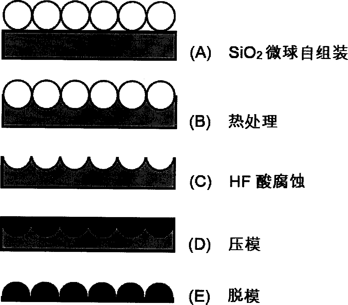
[0018] Example 1: Arranging submicron / micron SiO on the surface of polycarbonate polymer with high softening point and low elasticity by self-assembly technology 2 Microspheres, to obtain a large-area highly ordered two-dimensional single-layer microsphere array; then put it in an incubator for heat treatment at 140 ° C for 1 min; use HF acid solution to remove SiO 2 After microspheres, a large-area highly ordered two-dimensional concave lens array on the surface of polycarbonate and other polymers can be obtained; the above-mentioned concave lens array is used as a template to press on the surface of polymethyl methacrylate polymer with high light transmittance, and put Heat treatment at 80°C for 5 minutes in an incubator and demoulding to obtain a convex lens array on the surface of polymers such as polymethyl methacrylate or polystyrene;

Embodiment 2

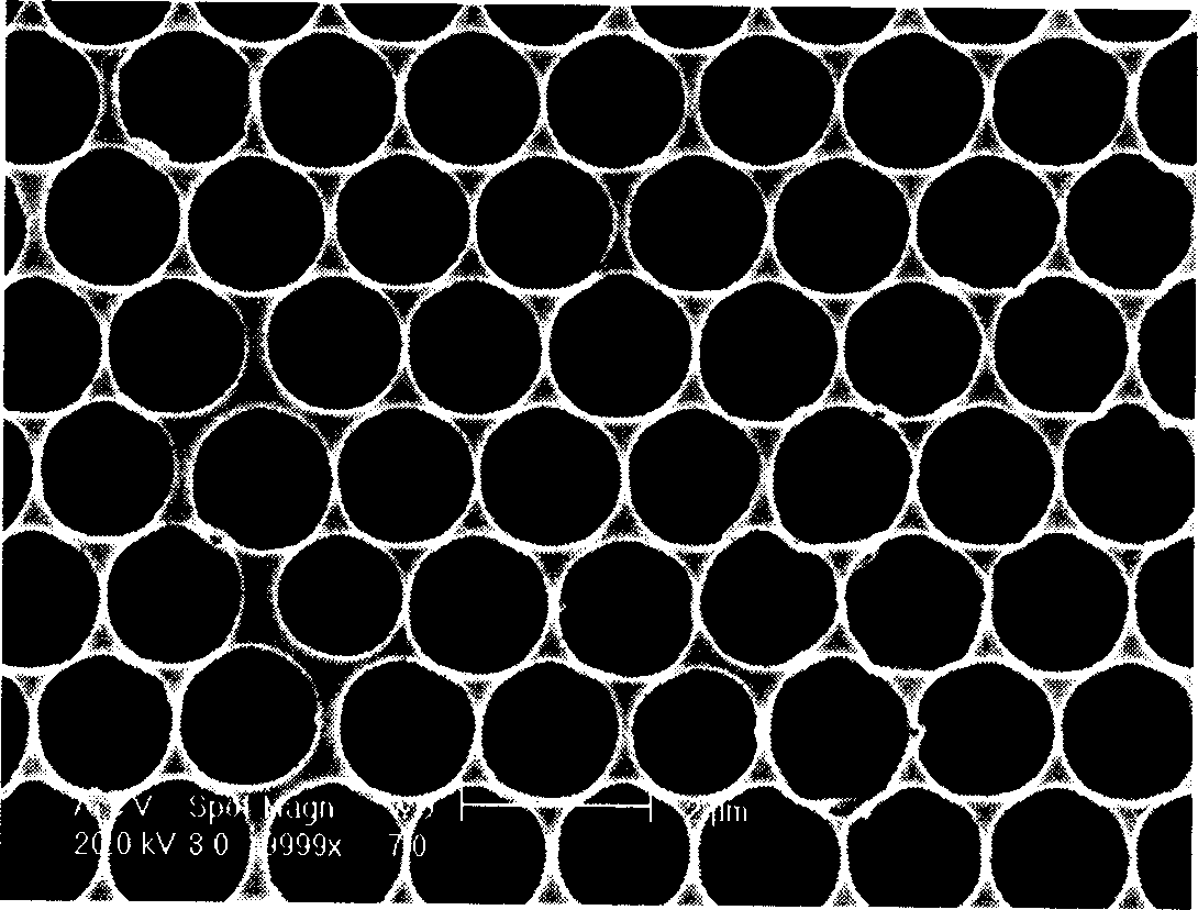
[0019] Embodiment 2: utilize self-assembly technology to SiO 2 The microspheres were arranged on the surface of polycarbonate, and then heat-treated at 180 °C for 24 h, and after natural cooling, the SiO 2 The template is removed to obtain a polycarbonate dimple lens array, see figure 2 .

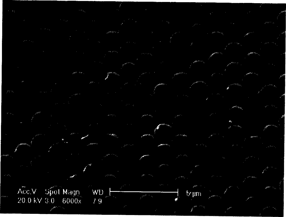
[0020] Place the above-mentioned micro-convex lens as a stamp on the surface of polymethyl methacrylate film, treat it at 130°C for 1 hour, and obtain a polymethyl methacrylate micro-convex lens array after demoulding, see image 3 .

Embodiment 3

[0021] Embodiment 3: the preparation process is the same as the embodiment, the difference is that the high softening point and low elasticity polymer is selected polyamide (or polyoxymethylene), and another polymer material with high light transmittance is polystyrene, the first heat treatment The temperature is 150°C, and the time is 10h; the second heat treatment temperature is 100°C, and the time is 30min. The result is the same.


PUM


Abstract

The present invention discloses the preparation of micron / submicron micro lens array on polymer surface and belongs to the field of nanometer / micron micro structure material and preparing technology. The preparation process is combination of self-assembling process and pressure molding process, and includes the first preparation of micron / submicron print die plate via combination of colloid crystal template and hot treatment technology, and the subsequent hot press demolding to prepare micron / submicron micro lens array. The present invention has the advantages of low cost, simple technological process and apparatus, capacity of mass production, high micro lens performance, etc.

Description

1. Technical field [0001] The invention relates to a method for preparing a polymer surface micron / submicron microlens array. 2. Background technology [0002] Fabrication of submicron / micron microlens arrays is a technology with important application background. Because microlens arrays can correct light beams, optical connections, and imaging, they have been widely used in digital cameras, liquid crystal displays, light-emitting diodes, microlithography, confocal microscopes, optical converters, and connectors. The current microlens preparation technology usually uses expensive micro-processing methods and methods such as polymer melting, wet etching, impression, and photolithography. Among them, the impression method can be mass-produced, but the mold usually uses high-cost and complex equipment Micro-processing technology has a long production cycle, which limits the reduction of its cost. 3. Contents of the invention [0003] 1. Purpose of the invention: The purpose...

Claims


Application Information

Patent Timeline
IPC IPC(8): B29D11/00B29C71/02B29K25/00B29K33/04B29K59/00B29K61/00B29K69/00B29K77/00
Inventor 王振林祝名伟闵乃本
Owner NANJING UNIV
Why Eureka
Try Eureka