Covalent layer-by-layer self-assembling process for constructing polymer film on planar substrate

A layer-by-layer self-assembly, polymer film technology, applied in chemical instruments and methods, lamination, layered products, etc., to achieve the effects of fast reaction speed, high temperature stability, and stable structure

Inactive Publication Date: 2006-05-17
ZHEJIANG UNIV
View PDF0 Cites 9 Cited by
  • Summary
  • Abstract
  • Description
  • Claims
  • Application Information

AI Technical Summary

Problems solved by technology

So far, there are no literature reports on this

Method used


Image

  • Covalent layer-by-layer self-assembling process for constructing polymer film on planar substrate
  • Covalent layer-by-layer self-assembling process for constructing polymer film on planar substrate
  • Covalent layer-by-layer self-assembling process for constructing polymer film on planar substrate

Examples


Embodiment 1

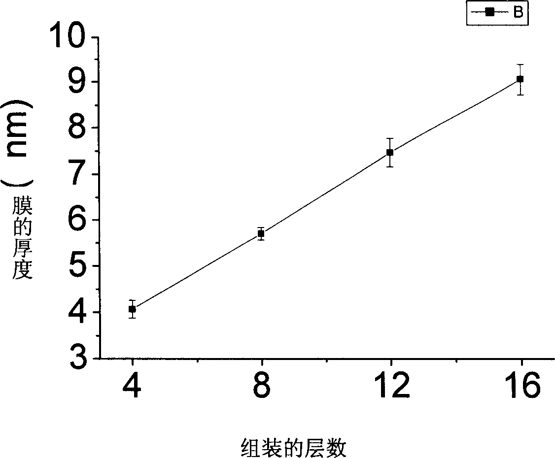
[0031] Soak the silicon chip in 40% hydrofluoric acid for 10 seconds, rinse it with water, dry it and suspend it above the dry toluene solution of 1% aminopropyltriethoxysilane, heat the solution to boil for 1 hour, Take it out to get an aminated silicon wafer. Put the aminated silicon wafer in a tetrahydrofuran solution of 4 mg / ml polyglycidyl methacrylate, and use an oil pump to evacuate until no bubbles are generated on the substrate. Then seal it, shake it at 20°C for 10 hours, then take it out, and wash it several times in ultrasonic with tetrahydrofuran. Put the silicon wafer into the aqueous solution of 4mg / ml polyallylamine, pump the vacuum with the water pump until no air bubbles are generated on the silicon wafer, then seal it, shake it at 20°C for 10 hours, then take it out, and immerse it in the ultrasonic wave with water. Wash several times. Repeat the above process to obtain polymer films assembled with 4 layers, 8 layers, 12 layers and 16 layers. The ellipsom...

Embodiment 2

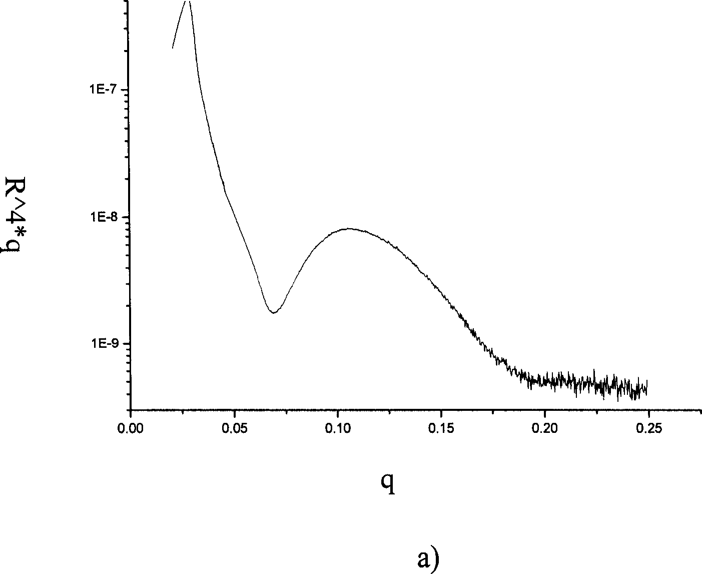
[0033] Soak the silicon chip in 10% hydrofluoric acid for 10 seconds, rinse it with water, dry it, suspend it above the dry toluene solution of 5% aminopropyltrimethoxysilane, heat it until the solution boils for 2 hours, take it out, Aminated silicon wafers were obtained. Put the aminated silicon wafer in a 1mg / ml tetrahydrofuran solution of polyglycidyl methacrylate, evacuate it with a water pump until no bubbles are generated on the silicon wafer, then seal it and shake it at 60°C for 0.5 hours , then removed and cleaned several times in ultrasonication with acetone. Put the silicon wafer into the aqueous solution of 1 mg / ml polyallylamine, pump the vacuum with water pump until no air bubbles are generated on the silicon wafer, then seal it, shake it at 60°C for 0.5 hours, then take it out, and use water to ultrasonically Wash several times. The above process was repeated 4 times to obtain an 8-layer polymer multilayer film. figure 2 (a) is the result of small-angle X-r...

Embodiment 3

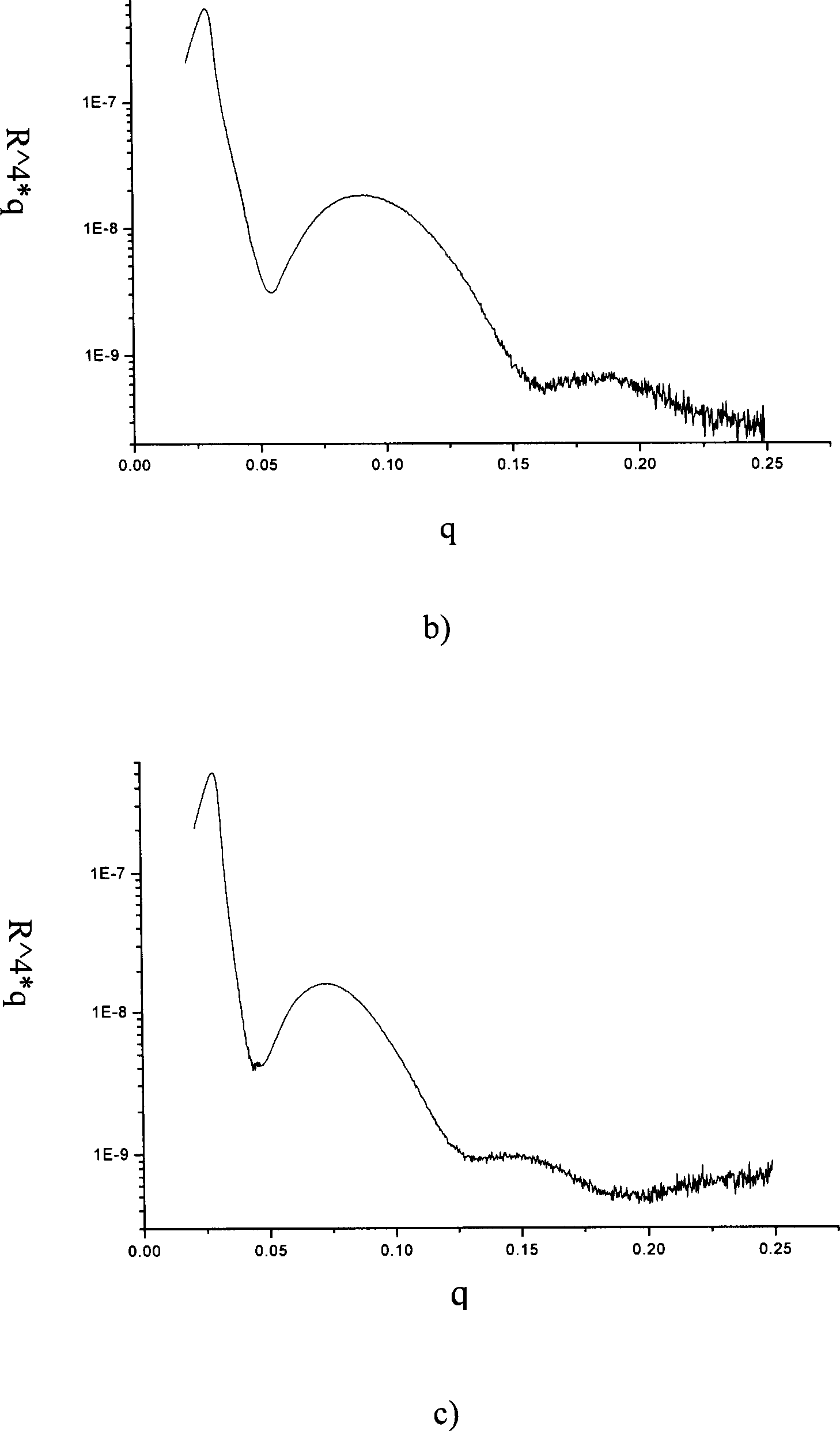
[0035] Soak the silicon chip in 20% hydrofluoric acid for 2 minutes, rinse with water, dry it, suspend it above the dry toluene solution of 10% aminopropyltrimethoxysilane, heat it until the solution boils for 5 hours, take it out, and get Aminated silicon wafers. Put the aminated silicon wafer in 8 mg / ml tetrahydrofuran solution of polyglycidyl methacrylate, vacuumize it with a water pump until no bubbles are generated on the silicon wafer, then seal it, and shake it at 60°C for 0.5 hours , and then removed and cleaned several times in ultrasonic with chloroform. Put the silicon wafer into the aqueous solution of 8 mg / ml polyallylamine, vacuumize it with an oil pump until no air bubbles are generated on the silicon wafer, then seal it, shake it at 80°C for 0.5 hours, then take it out, and use water to ultrasonically Wash several times. The above process was repeated 6 times to obtain a 12-layer polymer multilayer film. figure 2 (b) is the result of the small-angle X-ray d...


PUM


Abstract

The covalent layer-by-layer self-assembling process for constructing polymer film on planar substrate includes the first reaction of the substrate of surface aminated quartz or silicon chip and polymer with side radical containing epoxy group to form one layer of nanometer superthin film on the substrate by means of covalent bond; the subsequent reaction to polymer with side radical containing amino group to form one other layer of nanometer superthin film; and repeating the reaction with these two kinds of polymer solution to form superthin polymer film in multilayer structure, with each of the layers possessing thickness capable of being regulated in subnanometer level. The present invention has the features of simple technological process, adjustable film thickness, easy functionalizing, acid, base and organic solvent resistance of the film, high stability, etc. and is expected to find application in electronics, medicine, chemical and other fields.

Description

technical field [0001] The invention relates to a method for preparing a polymer ultra-thin film on the surface of a substrate. Specifically, the interaction of covalent bonds is used to form a polymer ultra-thin film with a multilayer structure through the layer-by-layer assembly reaction of two reactive polymers on the surface of the substrate. Background technique [0002] Constructing polymer films with specific structures and properties on the surface of substrates has important applications in the fields of sensors, microelectronics, food packaging, construction, and biotechnology. In these applications, these films are required to have uniformity, stability, reproducibility, adjustable film thickness and certain functionality. There are many ways to obtain polymer ultrathin films on the substrate surface, such as surface sol-gel, surface graft polymerization, surface coupling, microcontact printing, single-molecule self-assembly, LB film and layer-layer assembly, etc...

Claims


Application Information

Patent Timeline
Patent Type & Authority Applications(China)
IPC IPC(8): C08J5/24B32B27/00B32B38/08
Inventor 高长有封志强王志鹏沈家骢
Owner ZHEJIANG UNIV
Why Eureka
Try Eureka