

High purity gallium nitride nanometer line preparation method
A gallium nitride nanowire and high-purity technology, which is applied in the field of preparation of high-purity gallium nitride nanowires, can solve the problems affecting the product purity and yield, the surface is not smooth enough, and the raw material ratio of the preparation method is not strict enough, etc.
- Summary
- Abstract
- Description
- Claims
- Application Information
AI Technical Summary
Problems solved by technology
Method used
Image

Examples
Embodiment 1
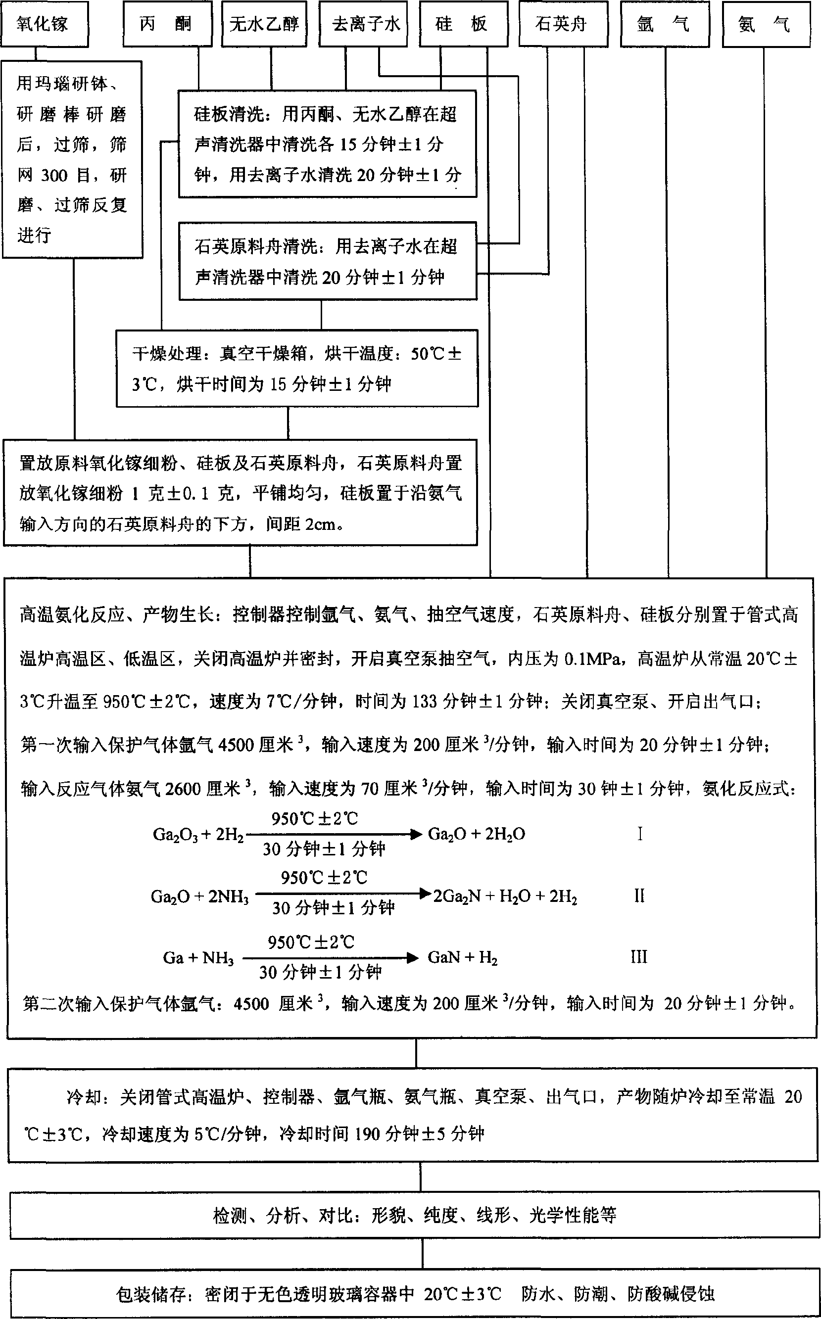
[0108] All production equipment are in quasi-working condition;
[0109] Accurately weigh according to the ratio, measure 1 gram of gallium nitride and 2600 cm of ammonia gas 3 , argon 9000 cm 3 , 20 ml of acetone, 20 ml of absolute ethanol, and 140 ml of deionized water;
[0110] Grinding and sieving: Grind and sieve the gallium oxide repeatedly to form a fine powder with a sieve of 300 mesh;
[0111] Ultrasonic cleaning of silicon plates: 20 ml of acetone, 20 ml of absolute ethanol, 40 ml of deionized water;
[0112] Ultrasonic cleaning of the quartz raw material boat: 100 ml of deionized water;
[0113] Drying treatment: silicon plates and quartz raw material boats are dried in a drying oven at a temperature of 50°C±3°C;
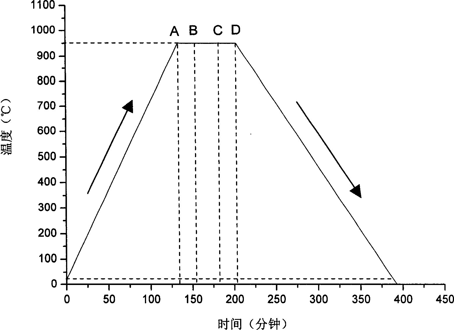
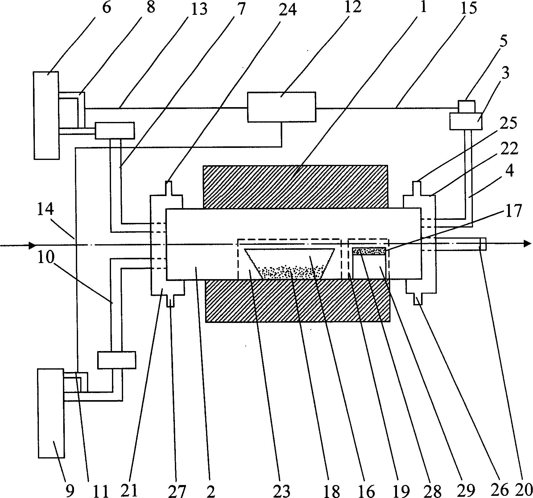
[0114] Place raw materials, silicon plate, and quartz raw material boat: gallium oxide fine powder is placed in the quartz raw material boat, the quartz raw material boat is placed in the high-temperature zone of the tubular high-temperature furnace, ...
PUM
| Property | Measurement | Unit |
|---|---|---|
| length | aaaaa | aaaaa |
Abstract
Description
Claims
Application Information