Equipment and method for measuring photoelectric performance of semiconductor nanometer structure

A technology of nanostructure and photoelectric properties, applied in the field of measurement of semiconductor nanomaterials, to achieve high comparability, high excitation intensity, elimination of shadowing and diffraction effects

Active Publication Date: 2010-05-05
SHANGHAI INST OF TECHNICAL PHYSICS - CHINESE ACAD OF SCI
View PDF5 Cites 0 Cited by
  • Summary
  • Abstract
  • Description
  • Claims
  • Application Information

AI Technical Summary

Problems solved by technology

[0004] However, with the development of semiconductor technology, especially the trend of opto-electronic integration, new requirements have been put forward for the detection technology of semiconductor nanomaterials, that is, the optoelectronic properties of nanomaterials and devices are required to be monitored. At present, there is no corresponding The device can perform measurements on this

Method used


Image

  • Equipment and method for measuring photoelectric performance of semiconductor nanometer structure
  • Equipment and method for measuring photoelectric performance of semiconductor nanometer structure
  • Equipment and method for measuring photoelectric performance of semiconductor nanometer structure

Examples


Embodiment Construction

[0027] The specific embodiment of the present invention is described in further detail below in conjunction with accompanying drawing:

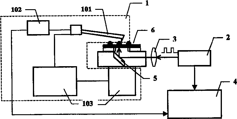
[0028] Measuring equipment of the present invention such as figure 1 As shown, it includes: a scanning probe microscope 1 , a pulsed laser 2 , a lens 3 , a mirror 5 and a photoelectric signal coupling measurement component 4 . The scanning probe microscope is a commercial multi-mode scanning probe microscope, which consists of a conductive micro-cantilever probe 101 , a weak current processing module 102 and a scanning system 103 .

[0029] Since the measurement process must ensure that the positioning accuracy of the needle tip reaches the nanometer level, and keep the drift speed below 0.05 nm / s during the measurement time, the scanning probe microscope must be placed on the anti-vibration table. The anti-vibration requirements of the anti-vibration table are When the vibration frequency is greater than 1 Hz, the root mean square value of ...


PUM


Abstract

A method for measuring photoelectric property of semiconductor nanostructure utilizes accurate space positioning and controlling ability of scan probe microscopic system to use conductive needle pointas nanoelectrode and to use back incoming mode to lead pulse laser into region to be tested of sample for exerting structure scanning on sample and simultaneously obtaining optical excited electricalproperty of specific nanoregion. The device for realizing said method is also disclosed.

Description

technical field [0001] The invention relates to the measurement of semiconductor nanomaterials, in particular to a device and method for measuring the photoelectric properties of semiconductor nanostructures. Background technique [0002] One of the most important development trends of semiconductor materials is the miniaturization of structure size, which makes us rely more on some high-resolution detection methods. [0003] Scanning probe microscopy has been widely used in the study of surface topography and electronic structure of various materials for more than 20 years since it came out. Among them, atomic force microscopy has unique advantages in morphology observation and surface modification because it does not require electrical conductivity of materials. It is very suitable for semiconductor materials with a large electrical conductivity span, and is a good tool for research and development and process testing. In recent years, in response to some special measurem...

Claims


Application Information

Patent Timeline
Patent Type & Authority Patents(China)
IPC IPC(8): G01N23/227G01N13/00G01N1/28
Inventor 陆卫李天信李志锋邵军陈平平李宁张波陈效双
Owner SHANGHAI INST OF TECHNICAL PHYSICS - CHINESE ACAD OF SCI
Why Eureka
Try Eureka