Method for producing polycrystalline thin film transistor

A polysilicon thin film and manufacturing method technology, applied in semiconductor/solid-state device manufacturing, semiconductor devices, electrical components, etc., can solve the problems of reduced productivity, uneven distribution of laser energy, increased manufacturing cost, etc., and achieve improved uniformity and high additional effect of value

Inactive Publication Date: 2006-08-23
IND TECH RES INST
View PDF0 Cites 5 Cited by
  • Summary
  • Abstract
  • Description
  • Claims
  • Application Information

AI Technical Summary

Problems solved by technology

However, the crystal grains of polysilicon formed by the above-mentioned solid phase crystallization method or direct vapor deposition method are quite small, with a particle size of only about 100nm. Therefore, the properties of polysilicon thin films formed by these methods are not good.
[0005] At present, the Excimer Laser Anneal (ELA) technology is most commonly used in the production of polysilicon thin films. Although the polysilicon grain size that can be obtained can reach about 600nm, for the development of higher performance Flat screens are still not enough
At the same time, the general existing excimer laser tempering technology must use high repetition rate irradiation to improve the shortcomings of uneven laser energy distribution and unstable energy output, so as to reduce the phenomenon of uneven grain size distribution.
[0006] Among them, the problem of uneven grain size distribution will directly damage the electrical uniformity of the components and the consistency of the threshold voltage or sub-threshold swing value between components, and affect the production quality of the display when it develops towards a large area.
In addition, the excimer laser tempering process irradiated at a high repetition rate will also lead to an increase in production costs and a decrease in productivity, which is even more unfavorable for mass production of large-area displays

Method used


Image

  • Method for producing polycrystalline thin film transistor
  • Method for producing polycrystalline thin film transistor
  • Method for producing polycrystalline thin film transistor

Examples


Embodiment 1

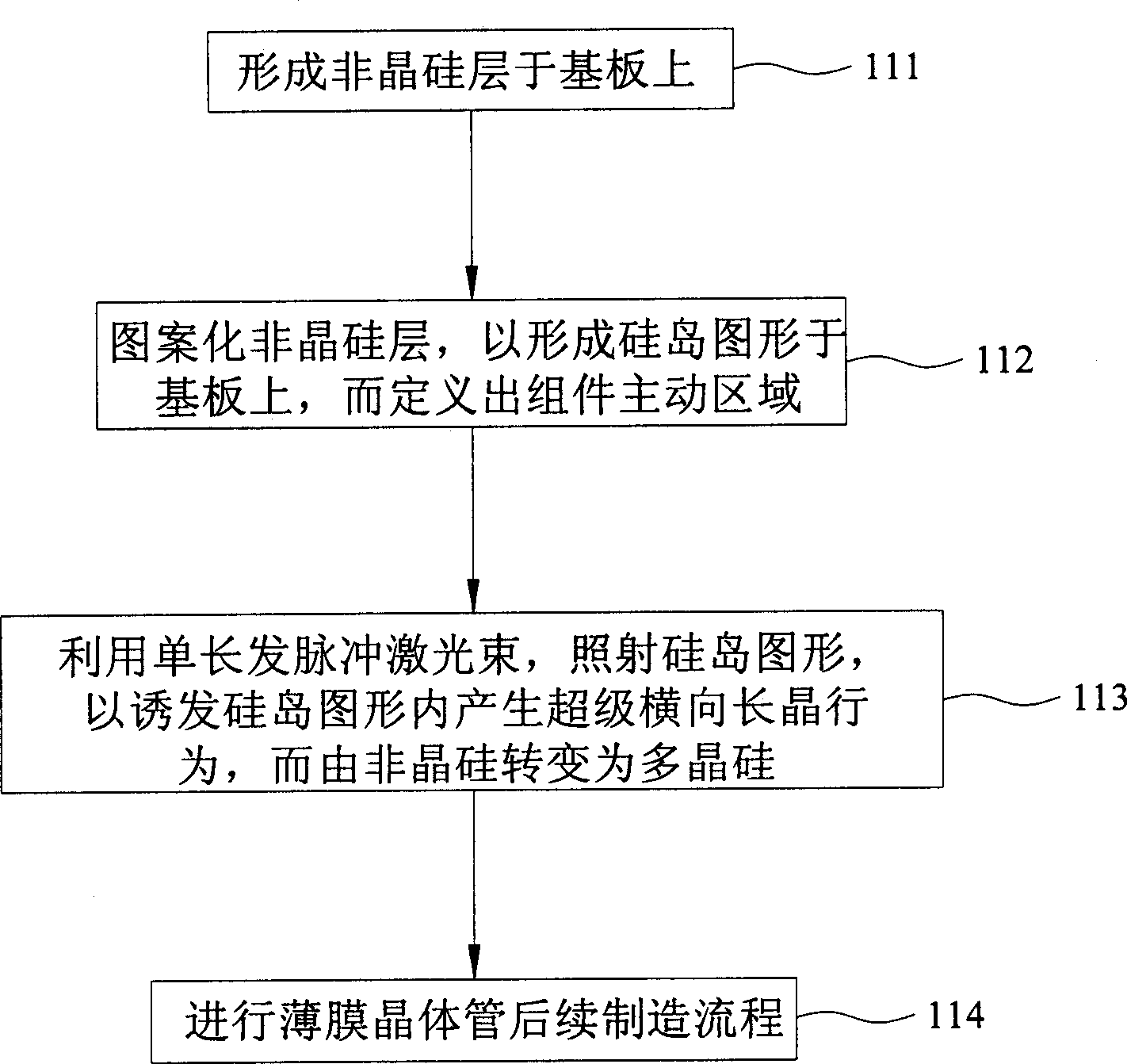
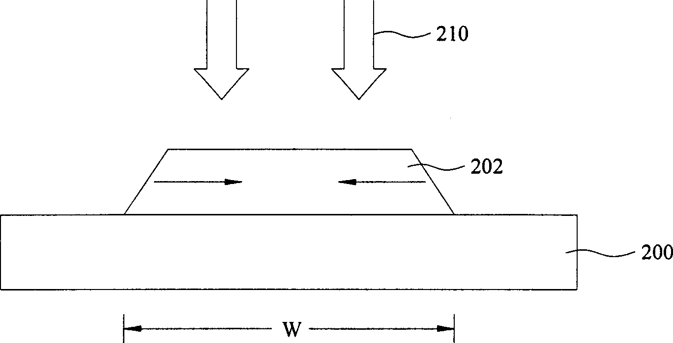
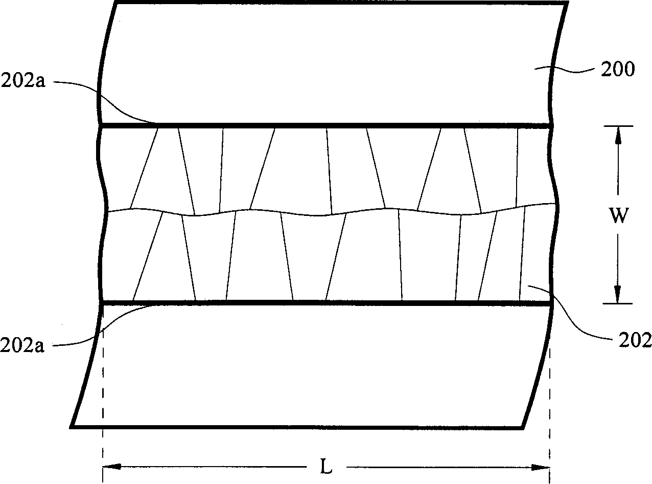
[0038] The invention discloses a method for manufacturing a polysilicon thin film transistor, with reference to figure 1 , Figure 2A as well as Figure 2B As shown, among them, figure 1 It is a flow chart of the steps of a method for manufacturing a polysilicon thin film transistor according to the first preferred embodiment of the present invention, and Figure 2A It is a schematic cross-sectional view of a part of the manufacturing process of a polysilicon thin film transistor according to the first preferred embodiment of the present invention. As for Figure 2B It is an enlarged top view diagram of the crystal structure in a polysilicon thin film transistor according to the first preferred embodiment of the present invention.

[0039] First, proceed figure 1 In the amorphous silicon layer forming step 111, then, the amorphous silicon layer is subjected to the patterning step 112 of defining the active area of ​​the component to form an amorphous silicon island pattern...

Embodiment 2

[0051] The present invention discloses another manufacturing method of a polysilicon thin film transistor. A transistor with a top gate structure is a preferred embodiment, with reference to image 3 as well as Figures 4A-4B shown. in, image 3 It is a flow chart of the steps of a method for manufacturing a polysilicon thin film transistor according to the second preferred embodiment of the present invention, and Figures 4A-4B It is a schematic cross-sectional view of the manufacturing process of a polysilicon thin film transistor according to the second preferred embodiment of the present invention.

[0052] First, proceed image 3 The formation step 311 of the buffer layer and the amorphous silicon layer, cooperates Figure 4A As shown, the buffer layer 401 and the amorphous silicon layer 402 are sequentially formed on the substrate 400 respectively; wherein, the substrate 400 is also made of glass, and the buffer layer 401 can be, for example, a silicon oxide film. N...


PUM


Abstract

Said polysilicon thin film transistor making method makes patterning to non-crystalline silicon layer after forming non-crystalline silicon layer on substrate to form silicon island graphic, advance defining out assembly active area. Then said method utilizes single shot long pulse laser bean to radiate silicon island graphic, to induce silicon island generating super transverse direction long glittering acting, converting non-crystalline silicon to polysilicon, finally according to sequence to proceed follow-up thin film transistor making process to complete polysilicon thin film transistor manufacture.

Description

technical field [0001] The present invention relates to a method for manufacturing polysilicon thin film transistors, and in particular to a method for manufacturing polysilicon thin films with regularly distributed super laterally grown crystal grains, so as to be applied to the manufacture of large-area thin film transistor displays. Background technique [0002] Polysilicon (poly-silicon) has been widely valued in the manufacture of thin-film transistors in recent years because of its electrical characteristics superior to amorphous silicon and its cost advantage lower than that of single-crystal silicon, especially in thin-film transistor-driven liquid crystal displays (TFT -LCD) applications. [0003] However, the grain size of polysilicon crystals directly has a great impact on electron mobility and component characteristics. Therefore, how to increase the crystal grain size of polysilicon to promote the improvement of the characteristics of thin film transistor compon...

Claims


Application Information

Patent Timeline
Patent Type & Authority Applications(China)
IPC IPC(8): H01L21/336H01L21/20H01L21/00
CPCH01L29/78696H01L21/02532H01L29/66757H01L21/02422H01L21/02686
Inventor 林家兴陈昱丞陈麒麟
Owner IND TECH RES INST
Why Eureka
Try Eureka