Processes for fabricating conductive patterns using nanolithography as a patterning tool

A nano and pattern technology, applied in conductive pattern formation, nanotechnology, nanotechnology, etc., can solve problems such as electrochemical bias limitation and metal processing difficulties

Inactive Publication Date: 2006-12-06
NANOINK INC
View PDF18 Cites 6 Cited by
  • Summary
  • Abstract
  • Description
  • Claims
  • Application Information

AI Technical Summary

Problems solved by technology

However, processing metals can be difficult, and manipulating them at the nanoscale is even more difficult
Many approaches are limited only to the level of microfabrication
Many methods are limited by the need for electrochemical bias or very high temperatures
Additionally, many methods are limited by the physical conditions of the deposition process, such as ink viscosity

Method used


Image

  • Processes for fabricating conductive patterns using nanolithography as a patterning tool
  • Processes for fabricating conductive patterns using nanolithography as a patterning tool
  • Processes for fabricating conductive patterns using nanolithography as a patterning tool

Examples


Embodiment approach

[0045] Especially in the prior application 09 / 866533 filed on May 24, 2001 (references 7 and 8, 2002 / 0063212 A1 published on May 30, 2002), the background of direct-write nano-etching printing is disclosed in detail Technology and methods, including various implementations, such as: background technology (pages 1-3); summary of the invention (pages 3-4); brief description of the drawings (pages 4-10); scanning probe tip Use of (pages 10-12); substrates (pages 12-13); patterned compounds (pages 13-17); implementation methods, including, for example, tip coating (pages 18-20); including nanoplotters Instrumentation (page 20-24); multilayer application and related printing and etching methods (page 24-26); resolution (page 26-27); matrix and combination matrix (page 27-30); Software and scales (pages 30-35, 68-70); kits and components including tips coated with hydrophobic compounds (pages 35-37); working examples (pages 38-67); corresponding claims And summary (pages 71-82); and att...

Embodiment 1

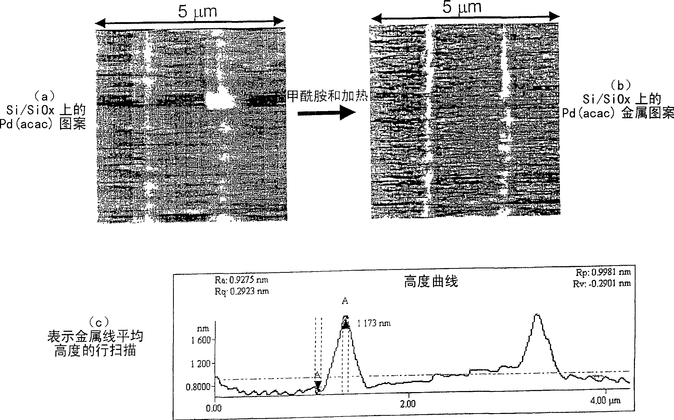
[0115] A specific example of this method is the use of DPN TM For printing or deposition patterning, palladium acetylacetonate dissolved in chloroform (1 mg / μl, usually requires an almost saturated ink solution) is patterned on oxidized silicon, glass or aminosilanized glass. After the dots are formed, a drop (1 microliter) of formamide is dropped on the horizontal substrate and heated to 150°C for 2 minutes. The resulting metal pattern remains stable to solvent (including water, alcohol and other non-polar organics) rinsing, and the salt pattern before reduction is removed by solvent rinsing. figure 1 Indicates that before using formamide and heat treatment ( figure 1 a) and after processing ( figure 1 b and figure 1 c) AFM image and pattern height scan.

Embodiment 2

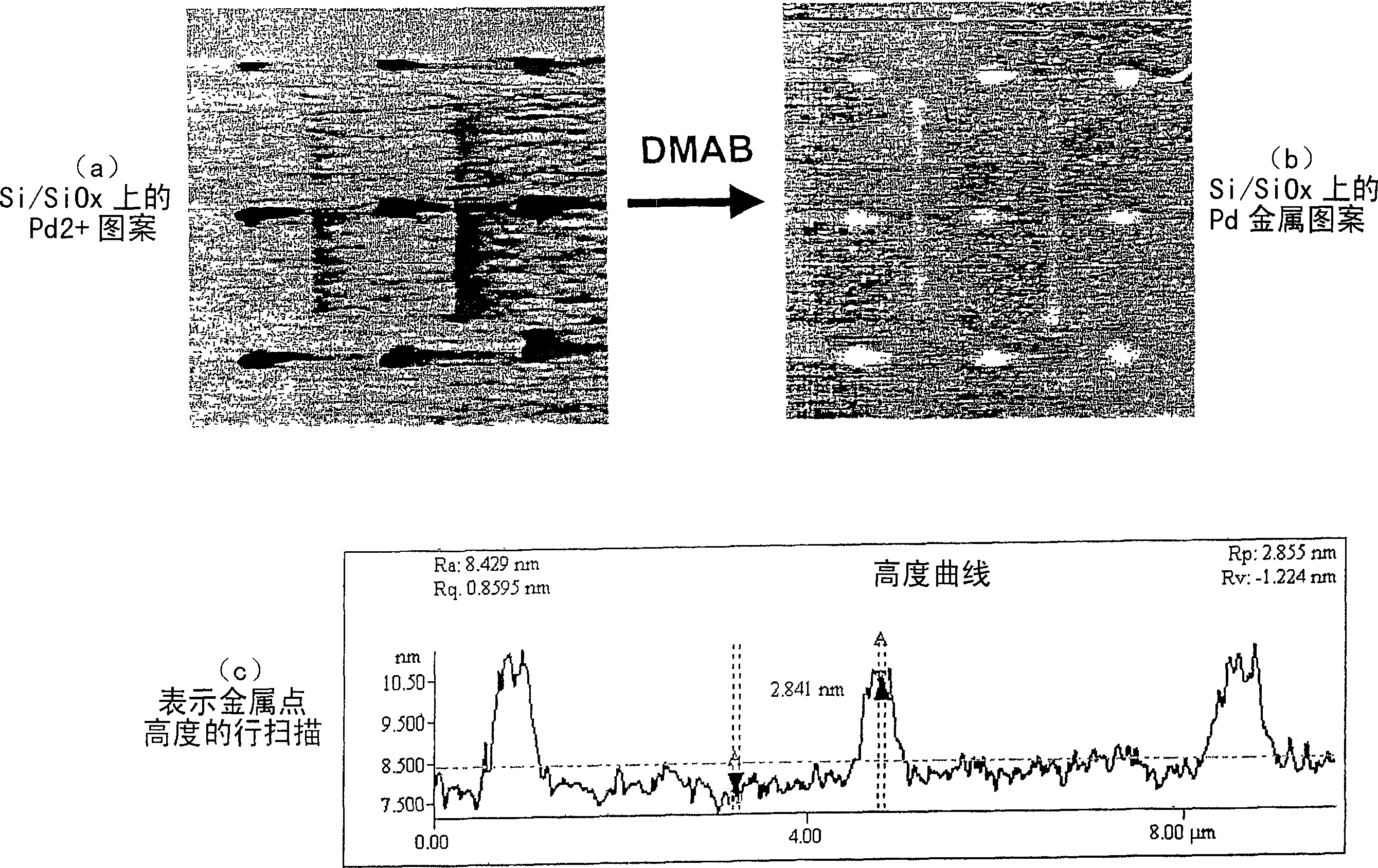
[0117] Palladium nanopatterns were deposited by DPN printing and metallized by steam reduction. The DPN ink was patterned on silicon oxide using DPN technology, and the ink consisted of a dimethylformamide solution of palladium acetate. The DPN pen used is a silicon nitride probe coated with gold. This method is very suitable for the use of aluminum-plated DPN probes, because the aluminum coating does not directly reduce the metal salt to the cantilever, while the gold-plated probe may directly reduce the metal salt to the cantilever. Before patterning, the silicon / silicon oxide wafer was sonicated and cleaned in microporous water for 5 minutes. The patterned substrate was placed vertically in a conical polyethylene tube, and 10 microliters of formamide liquid was placed at the bottom of the tube. The tube was placed on a heater and heated at 80°C for 30 minutes, so that the steam caused reduction of the metal precursor. Since this method protects the metal pattern on the substrat...


PUM

PropertyMeasurementUnit
thicknessaaaaaaaaaa
thicknessaaaaaaaaaa

Abstract

Nanolithographic deposition of metallic nanostructures using coated tips for use in microelectronics, catalysis, and diagnostics. AFM tips can be coated with metallic precursors and the precursors patterned on substrates. The patterned precursors can be converted to the metallic state with application of heat. High resolution and excellent alignment can be achieved.

Description

Background technique [0001] Many important applications in bioengineering, diagnostics, microelectronics, and nanotechnology require the nanostructure of metals, which is a basic type of matter. For example, better microelectronics needs to provide smaller and faster computer chips and circuit boards, and metals can provide the required conductivity to form circuits. Metals can also be used as catalysts. However, processing metals may be difficult, and operations at the nanometer level are even more difficult. Many methods are limited to the level of micro manufacturing. Many methods are limited due to the need for electrochemical bias or very high temperature. In addition, many methods are also limited by the physical conditions of the deposition process, such as ink viscosity. There is a need for a better method of fabricating metal nanostructures that can provide alignment capabilities for thin films and wires, high resolution, and versatility. Summary of the invention [0002...

Claims


Application Information

Patent Timeline
Patent Type & Authority Applications(China)
IPC IPC(8): H01L21/44B32B3/00B32B27/14B05D1/36B05D5/12B01JC23C18/08C23C18/16C23C18/28G01Q60/00G01Q70/00G01Q80/00H01L21/288H01L21/768H05K3/10H05K3/12
CPCC23C18/06C23C18/08C23C18/1678C23C18/161C23C18/1666H05K3/105C23C18/1603B82Y40/00B82Y10/00H05K3/1241G03F7/0002C23C18/1612C23C18/1667C23C18/28Y10S438/929H01L21/288H01L21/76838C23C18/1658H01L21/44H01L21/4763B05D1/36B05D5/12
Inventor 小珀西·范登·克罗克利内特·德默斯纳比尔·A.·阿姆鲁罗伯特·埃勒加尼安
Owner NANOINK INC
Why Eureka
Try Eureka