Method for MOCVD growth nitride light-emitting diode structure extension sheet
A technology of light-emitting diodes and epitaxial wafers, which is applied in the direction of electrical components, circuits, semiconductor devices, etc., can solve problems that affect the quality of epitaxial layers, device performance, high forward operating voltage, and increase operating voltage, so as to improve quality and device performance. High saturation speed, effect of reducing resistance
- Summary
- Abstract
- Description
- Claims
- Application Information
AI Technical Summary
Problems solved by technology
Method used
Image
Examples
Embodiment 1
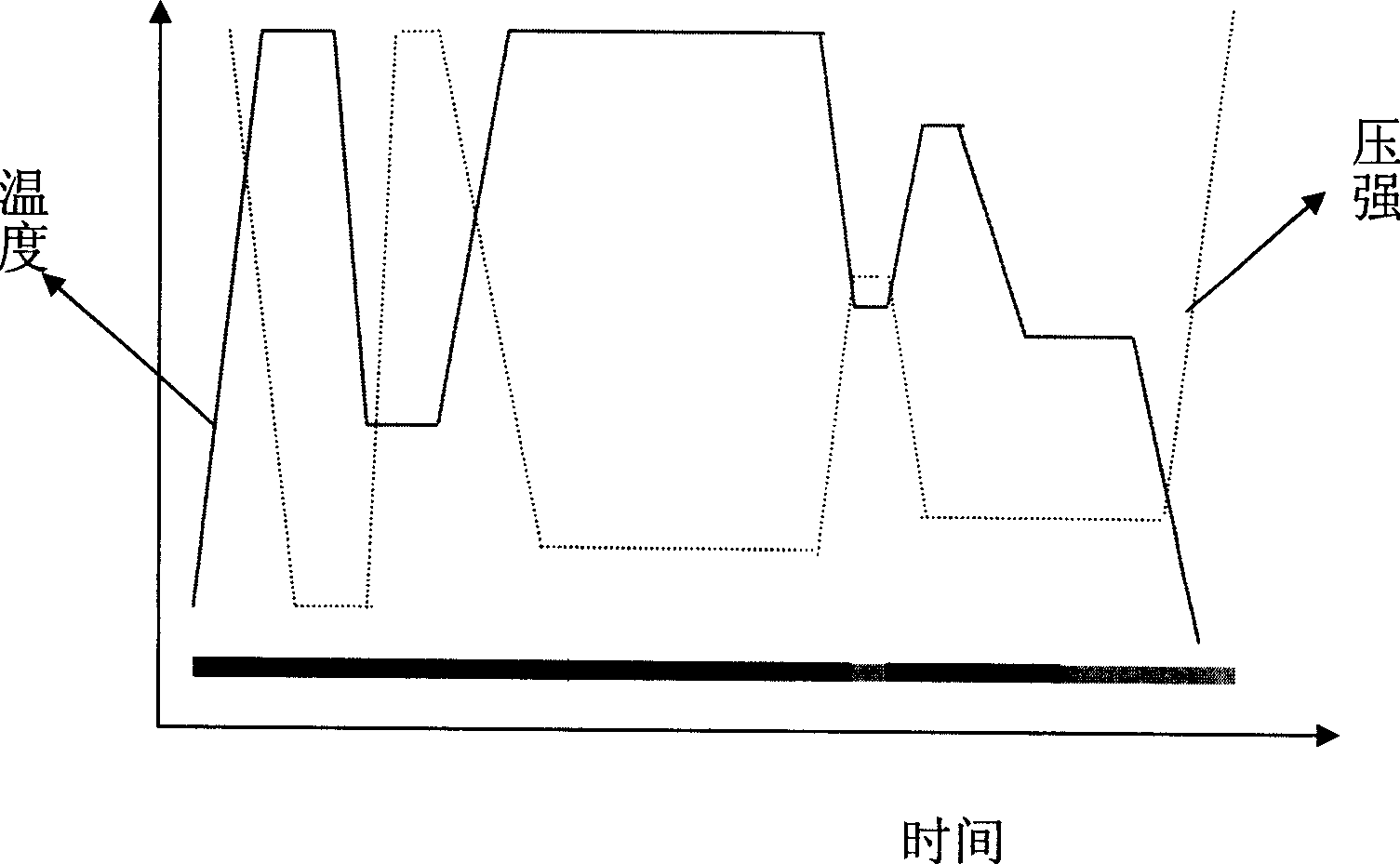
[0017] GaN-based ultra-high-brightness LED structure epitaxial wafers were grown using MOCVD 2000HT from AXTRON, Germany. The substrate is (0001) sapphire (Al 2 o 3 ). Such as figure 1 As shown, first, the sapphire substrate 1 is heated to 1200°C in the MOCVD reaction chamber, and treated at high temperature under hydrogen for 10 minutes; then the temperature is lowered to 490-550°C to grow the GaN nucleation layer 2, about 30 nanometers, and the TMGa flow rate is 1 *10 -4 mol / min, NH 3 The flow rate is 15 liters / minute; thereafter, the growth temperature is raised to 1160° C. to anneal the GaN nucleation layer 2, and the annealing time is between 4 and 8 minutes; after annealing, the growth temperature is raised to 1180° C. to start Epitaxial growth of the GaN buffer layer, a GaN buffer layer with a thickness of 3.5 microns is grown at a uniform speed, of which 1 micron is the unintentionally doped GaN buffer layer 3, and the last 2.5 microns is the Si-doped GaN buffer l...
Embodiment 2
[0019] GaN-based ultra-high brightness LED structure epitaxial wafers were grown by using MOCVD Gailla epitaxy of Veeco in the United States. Among them, the substrate is (0001) sapphire (Al 2 o 3 ). Such as figure 1 As shown, first, the sapphire substrate 1 is heated to 1100°C in the MOCVD reaction chamber, and treated at high temperature under hydrogen for 10 minutes; then the temperature is lowered to 490-550°C to grow the GaN nucleation layer 2, about 20 nanometers, and the TMGa flow rate is 2 *10 -4 mol / min, NH 3 The flow rate is 40 liters / minute; thereafter, the growth temperature is raised to 1060°C to anneal the nucleation layer 2, and the annealing time is between 8 minutes; after annealing, the growth temperature is raised to 1080°C, and epitaxial growth of GaN is started Buffer layer, a GaN buffer layer with a thickness of 3.5 microns grown at a uniform speed, of which 1 micron is an unintentionally doped GaN buffer layer 3, and the last 2.5 microns is a Si-dop...
PUM
| Property | Measurement | Unit |
|---|---|---|
| Thickness | aaaaa | aaaaa |
Abstract
Description
Claims
Application Information


