Check patentability & draft patents in minutes with Patsnap Eureka AI!

Method of fast preparing and screening nanometer IIB semiconductor light-emitting material

A nano-luminescent material and semiconductor technology, applied in the direction of luminescent materials, chemical instruments and methods, can solve the problems of long cycle, low output, and large contingency of luminescent performance, and achieve the improvement of fluorescence intensity, reduction of test cost, and shortening of screening cycle. Effect

Inactive Publication Date: 2007-01-03
TONGJI UNIV
View PDF0 Cites 0 Cited by
  • Summary
  • Abstract
  • Description
  • Claims
  • Application Information

AI Technical Summary

Problems solved by technology

[0005] So far, only the traditional "stir-frying" synthesis method is used to prepare nanomaterials and study their luminescent properties, which have disadvantages such as large chance, low output and long cycle.

Method used


Image

  • Method of fast preparing and screening nanometer IIB semiconductor light-emitting material
  • Method of fast preparing and screening nanometer IIB semiconductor light-emitting material
  • Method of fast preparing and screening nanometer IIB semiconductor light-emitting material

Examples


Embodiment 1

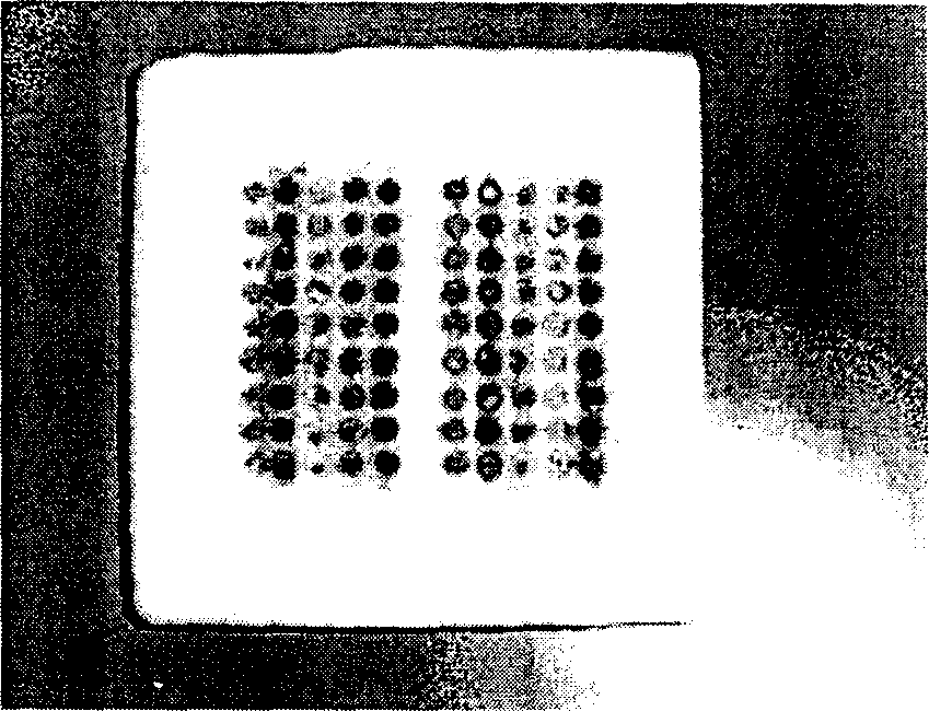
[0032] (1) As shown in Table 1, use the orthogonal design method to design 9 kinds of silver-doped zinc sulfide nano-crystallite schemes, and comprehensively consider the factors that affect the morphology and performance of the product;

[0033] No.

c(M)

n (zinc nitrate: silver nitrate)

n (zinc nitrate + silver nitrate): n (sodium sulfide)

n(SDS):n(sodium sulfide)

1

2

0.1

0.1

5∶5

5∶3

1∶1

1∶0.9

1∶48

1∶50

3

4

5

6

7

8

9

0.1

0.2

0.2

0.2

0.5

0.5

0.5

5∶1

5∶5

5∶3

5∶1

5∶5

5∶3

5∶1

1∶0.8

1∶0.9

1∶0.8

1∶1

1∶0.8

1∶1

1∶0.9

1∶52

1∶50

1∶52

1∶48

1∶52

1∶48

1∶50

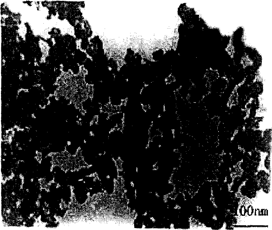
[0034] (2) Prepare certain concentrations of zinc nitrate, silver nitrate, sodium sulfide and sodium dodecyl sulfate (SDS) according to the requirements of Table 1 and fill them in beakers respectively; ...

Embodiment 2

[0040] (1) As shown in Table 2, nine kinds of manganese-doped cadmium sulfide nanocrystallite schemes were designed by using the orthogonal design method, and the factors affecting the product morphology and performance were comprehensively considered;

[0041] No.

c(M)

n (cadmium nitrate: manganese nitrate)

n (cadmium nitrate + manganese nitrate): n (sodium sulfide)

n(SDS):n(sodium sulfide)

1

2

3

4

5

6

7

0.1

0.1

0.1

0.2

0.2

0.2

0.5

5∶5

5∶3

5∶1

5∶5

5∶3

5∶1

5∶5

1∶1

1∶0.9

1∶0.8

1∶0.9

1∶0.8

1∶1

1∶0.8

1∶48

1∶50

1∶52

1∶50

1∶52

1∶48

1∶52

8

9

0.5

0.5

5∶3

5∶1

1∶1

1∶0.9

1∶48

1∶50

[0042] (2) Prepare certain concentrations of soluble cadmium nitrate, manganese nitrate, sodium sulfide and sodium dodecyl sulfate (SDS) according to the requirements of Table 2 and fill t...

Embodiment 3

[0048] (1) As shown in Table 3, nine kinds of manganese-doped cadmium sulfide nanocrystallite schemes were designed by using the orthogonal design method, and the factors affecting the product morphology and performance were comprehensively considered;

[0049] No.

c(M)

n (cadmium acetate: manganese acetate)

n (cadmium acetate + manganese acetate): n (sodium sulfide)

n(SDS):n(sodium sulfide)

1

2

3

4

5

6

7

8

9

0.1

0.1

0.1

0.2

0.2

0.2

0.5

0.5

0.5

5∶5

5∶3

5∶1

5∶5

5∶3

5∶1

5∶5

5∶3

5∶1

1∶1

1∶0.9

1∶0.8

1∶0.9

1∶0.8

1∶1

1∶0.8

1∶1

1∶0.9

1∶48

1∶50

1∶52

1∶50

1∶52

1∶48

1∶52

1∶48

1∶50

[0050] (2) Prepare a certain concentration of soluble cadmium acetate, manganese acetate, sodium sulfide and sodium dodecyl sulfate (SDS) according to the requirements of Table 3 and fill them in beakers re...


PUM

PropertyMeasurementUnit
particle diameteraaaaaaaaaa
sizeaaaaaaaaaa
particle diameteraaaaaaaaaa

Abstract

The present invention belongs to the field of nanometer light-emitting material technology, and is especially method of fast preparing and screening nanometer IIB semiconductor light-emitting material. The method includes designing 9 nanometer IIB semiconductor light-emitting materials by means of orthogonal design method; compounding solution in certain concentration and of soluble IIB metal salts, sodium sulfide and sodium dodecyl sulfate; titrating in parallel while stirring; washing to obtain the required products; and screening the products with transmission electron microscope and fluorescence instrument. The present invention has low cost, simple process, fast preparation and no pollution, and may be used widely for preparing and screening target product chemically.

Description

technical field [0001] The invention belongs to the technical field of nano-luminescent materials, in particular to a method for rapidly preparing and screening IIB group semiconductor nano-luminescent materials. Background technique [0002] Today, with the rapid development of modern high-tech and high-tech industries, there is an increasing demand for new materials with specific functions. Therefore, accelerating the development of new materials is a major challenge facing the scientific community today. The chemical industry is undergoing a comprehensive structural adjustment in the global economy and sustainable development. Although the composition and structure of compounds are rich and diverse, it is still difficult to find new substances with specific functions. The traditional "stir-frying style" synthesis strategy is inefficient, which makes the discovery and optimization of new materials have disadvantages such as high cost, long cycle, low output and large chanc...

Claims


Application Information

Patent Timeline
Patent Type & Authority Applications(China)
IPC IPC(8): C09K11/54
Inventor 吴庆生张晓喻丁亚平
Owner TONGJI UNIV
Features
  • R&D
  • Intellectual Property
  • Life Sciences
  • Materials
  • Tech Scout
  • Unparalleled Data Quality
  • Higher Quality Content
  • 60% Fewer Hallucinations
Learn More