A conductive electrode powder, a method for preparing the same, preparing method of electrode of plasma display and plasma display
A plasma display screen and electrode powder technology, which is applied in the direction of alternating current plasma display panels, gas discharge electrodes, and electrode system manufacturing, and can solve problems that do not involve the corrosion resistance of the electrodes themselves
- Summary
- Abstract
- Description
- Claims
- Application Information
AI Technical Summary
Problems solved by technology
Method used
Image
Examples
preparation example Construction
[0061] As the conductive metal particles used in the production method for forming the conductive powder for electrodes, any metal particles having excellent conductivity can be used, but it is preferable to use metal particles selected from silver (Ag), gold, palladium, platinum, copper, aluminum, At least one substance in the group consisting of tungsten, molybdenum and alloys formed by two or more of the aforementioned metals. Among them, silver (Ag) is most preferable because of its excellent conductivity.
[0062] In addition, the inorganic oxide particles preferably have an average diameter in the range of 1 μm or less, more preferably 10 nm to 500 nm, further preferably 10 nm to 50 nm. The smaller the average diameter of the inorganic oxide particles, the more preferable. When it is larger than 500 nm, it is difficult to obtain a uniform coating; and when it is smaller than 10 nm, it is difficult to obtain inorganic oxide particles having such a small average diameter....
Embodiment 1
[0096] 100 parts by weight of a silica solution (water glass) (manufactured by FERRO Co.) containing 15 wt % of silica particles with an average particle diameter of 50 nm was mixed with 300 parts by weight of amorphous silver (Ag) powder (DOWA Hightech Co., Ltd. ., spherical particle shape) mixing. Then, the mixture was stirred, sprayed, and baked at 580° C. for 60 minutes to prepare conductive electrode powder.
[0097] Fig. 6 is a scanning electron microscope (SEM) photograph of a conductive electrode powder with a silica coating.
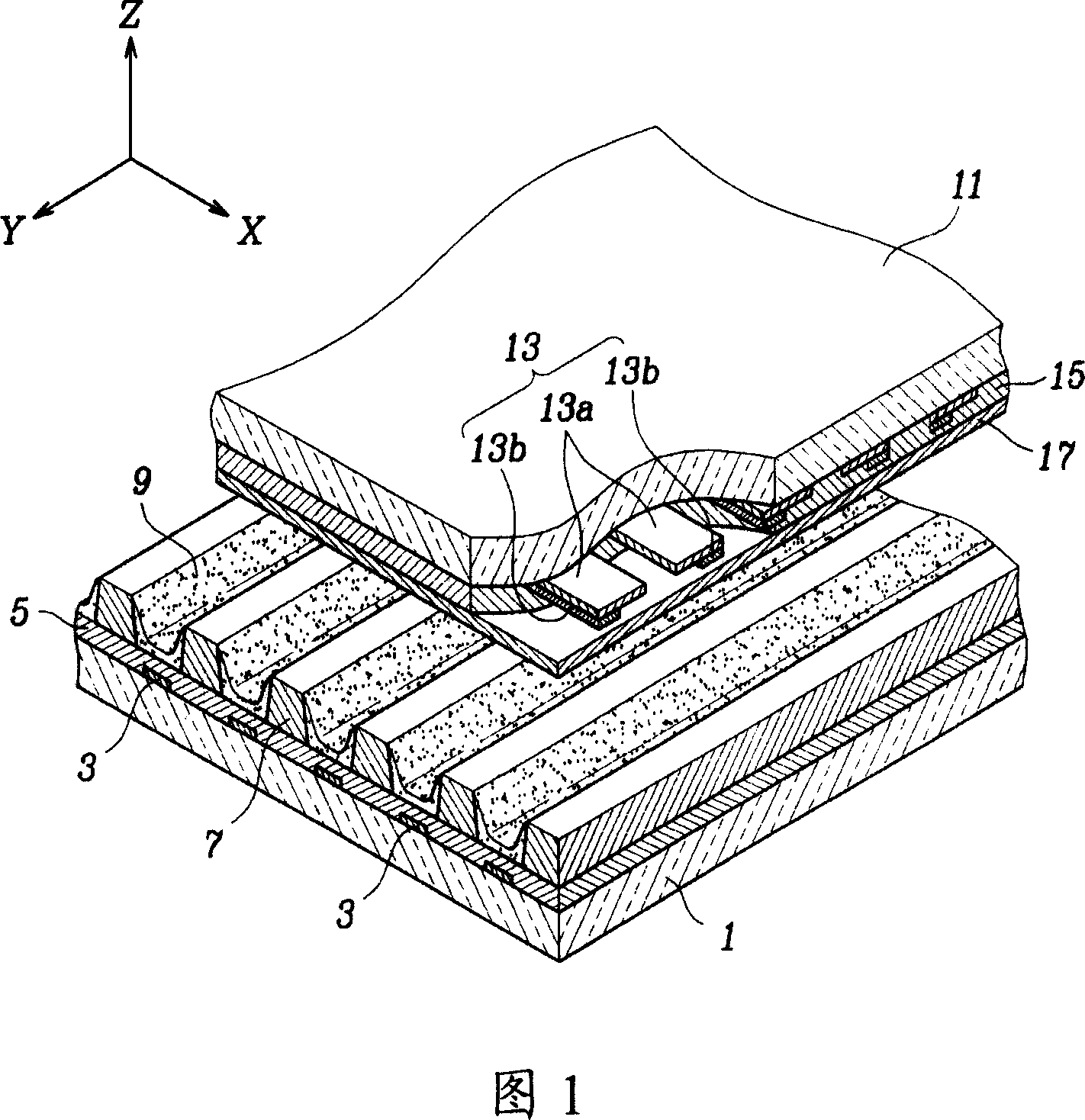
[0098] Except that 29.8wt% of the photosensitive medium prepared according to Comparative Example 1 and 65wt% of the conductive powder prepared according to Example 1, 3wt% of PbO, and 2wt% of B 2 o 3 Address electrodes and a plasma panel were produced in the same manner as in Comparative Example 1 except that the slurry was prepared by mixing with 0.2 wt% of silica.
Embodiment 2
[0100] Except that a photosensitive medium was prepared by mixing 5 wt % of a silica solution (water glass) (manufactured by Ferro Co.) containing 15 wt % of silica particles having an average particle diameter of 50 nm and 95 wt % of the photosensitive medium prepared according to Comparative Example 1 Except for the medium, address electrodes and a plasma panel were manufactured in the same manner as in Comparative Example 1.
[0101] FIG. 7 is a scanning electron microscope (SEM) photograph of the surface of the address electrode fabricated according to Example 2 after being baked.
PUM
| Property | Measurement | Unit |
|---|---|---|
| particle size | aaaaa | aaaaa |
| thickness | aaaaa | aaaaa |
| diameter | aaaaa | aaaaa |
Abstract
Description
Claims
Application Information
 - R&D
- Intellectual Property
- Life Sciences
- Materials
- Tech Scout
- Unparalleled Data Quality
- Higher Quality Content
- 60% Fewer Hallucinations
Browse by: Latest US Patents, China's latest patents, Technical Efficacy Thesaurus, Application Domain, Technology Topic, Popular Technical Reports.
© 2025 PatSnap. All rights reserved.Legal|Privacy policy|Modern Slavery Act Transparency Statement|Sitemap|About US| Contact US: help@patsnap.com


