H20 plasma and h20 vapor methods for releasing charges and use thereof

A plasma and charge technology, applied in the manufacture of circuits, electrical components, semiconductor/solid-state devices, etc., can solve the problems of general products without structure and inconvenience

Inactive Publication Date: 2007-04-04
TAIWAN SEMICON MFG CO LTD
View PDF0 Cites 6 Cited by
  • Summary
  • Abstract
  • Description
  • Claims
  • Application Information

AI Technical Summary

Problems solved by technology

[0007] It can be seen that the above-mentioned existing method for releasing the charge accumulated on the surface of the wafer obviously still has inconvenience and defects in use, and needs to be further improved urgently.
In order to solve the above-mentioned problems, the relevant m

Method used


Image

  • H20 plasma and h20 vapor methods for releasing charges and use thereof
  • H20 plasma and h20 vapor methods for releasing charges and use thereof
  • H20 plasma and h20 vapor methods for releasing charges and use thereof

Examples


Embodiment Construction

[0074] In order to further illustrate the technical means and effects that the present invention adopts to achieve the intended purpose of the invention, below in conjunction with the accompanying drawings and preferred embodiments, the use H proposed according to the present invention 2 O plasma and H 2 The method for releasing charge by O vapor and its application, its specific implementation, structure, characteristics and efficacy are described in detail below.

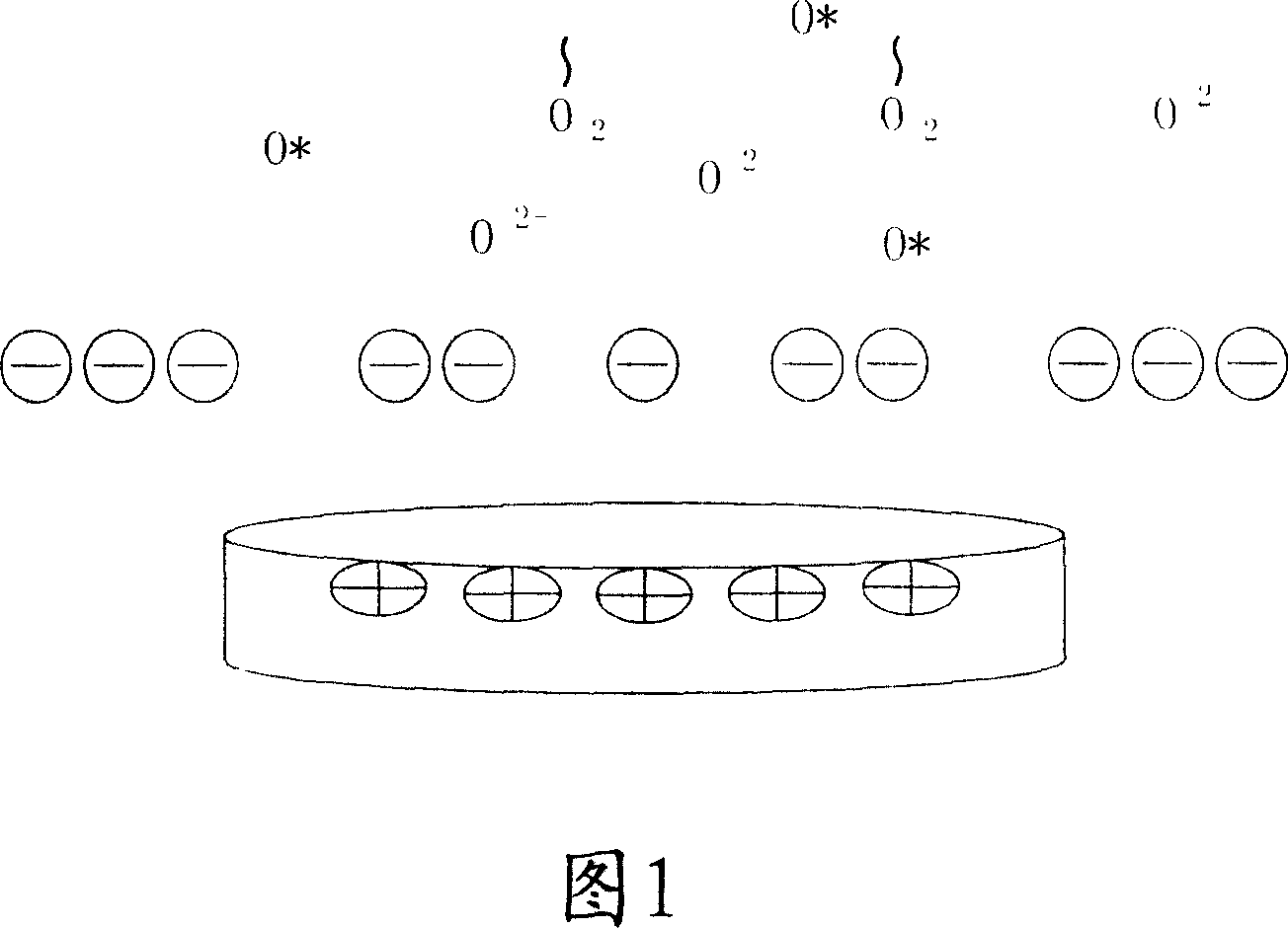
[0075] The disclosed in-situ methods are used to remove photoresist layers from a substrate or wafer without accumulating charge on the substrate or wafer and / or removing Or release charge accumulated by one or more integrated circuit construction processes. This approach eliminates or substantially reduces charges that can exacerbate electrochemical problems. Electrochemical issues include pad pitting, galvanic metal corrosion, tungsten corrosion, low-quality gate oxide, and other electrochemical issues.

[00...


PUM


Abstract

An in-situ performed method utilizing a pure H2O plasma to remove a layer of resist from a substrate or wafer without substantially accumulating charges thereon. Also, in-situ performed methods utilizing a pure H2O plasma or a pure H2O vapor to release or remove charges from a surface or surfaces of a substrate or wafer that have accumulated during one or more IC fabrication processes.

Description

technical field [0001] The invention relates to a manufacturing method of a semiconductor element, in particular to a method for releasing electric charge from a wafer. Background technique [0002] Integrated circuits are well known to those skilled in the art and typically include complete electronic circuits constructed on a single wafer. Integrated circuits are constructed using many different processes. These processes include oxidation, lithography, etching, ion doping, and metallization. During the process, the charge accumulated on the surface of the wafer can degrade the oxidation quality of the gate and / or dielectric layer, and / or change the parameters of the device. [0003] For example, a photoresist pattern layer defined by photolithography is used as a mask for etching the lower layer of the wafer. The photoresist layer after etching, such as photoresist or E-Beam Resist, is usually removed in an oxygen plasma process. In this oxygen plasma process, the waf...

Claims


Application Information

Patent Timeline
IPC IPC(8): H01L21/00G03F7/36G03F7/42
Inventor 李元榜吴子扬潘昇良林耀辉赖育志陈德芳林佩璇吴善华刘鸿兴
Owner TAIWAN SEMICON MFG CO LTD
Why Eureka
Try Eureka