Technique for nanometer grade super smooth processing gallium phosphide wafer

A processing technology, gallium phosphide technology, applied in metal processing equipment, manufacturing tools, grinding devices, etc., can solve the problems of complex processing technology and low processing quality of gallium phosphide, save processing time, simplify processing procedures, improve quality effect

Inactive Publication Date: 2007-04-18
周海
View PDF0 Cites 19 Cited by
  • Summary
  • Abstract
  • Description
  • Claims
  • Application Information

AI Technical Summary

Problems solved by technology

[0004] In order to overcome the problems of complex and low processing quality of the existing gallium phosphide processing technology, the present invention proposes a new gallium phosphide processing technology, which can simplify the process of gallium phosphide wafers and improve the processing quality of gallium phosphide wafers

Method used


Image

  • Technique for nanometer grade super smooth processing gallium phosphide wafer
  • Technique for nanometer grade super smooth processing gallium phosphide wafer
  • Technique for nanometer grade super smooth processing gallium phosphide wafer

Examples


Embodiment Construction

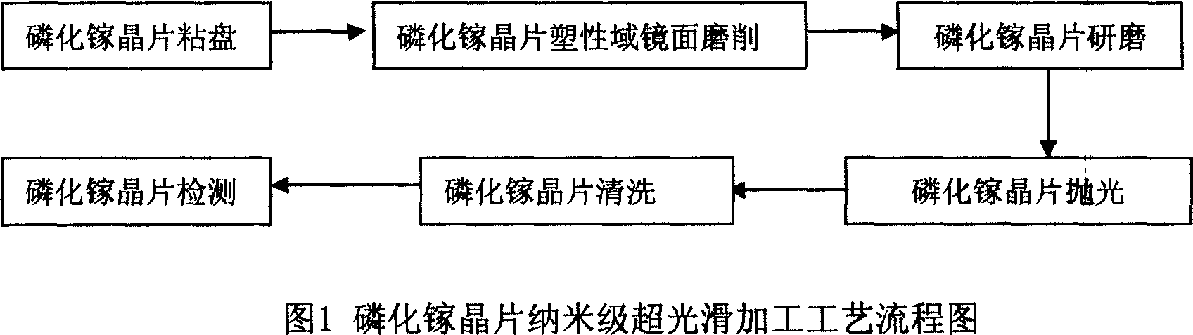
[0025] 1. First round the gallium phosphide ingot, and then slice it;

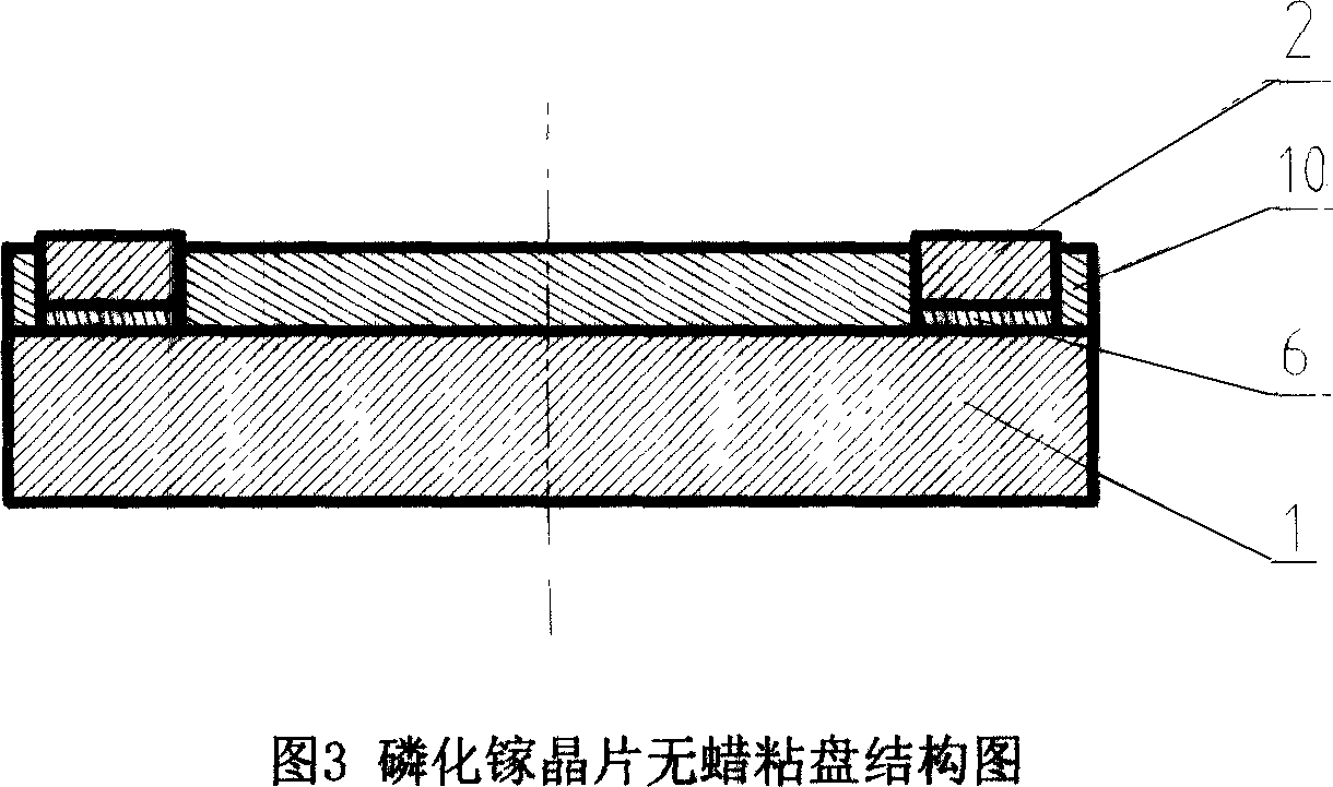
[0026] 2. Adsorb the gallium phosphide wafer into the carrier plate;

[0027] 3. On a high-rigidity grinding machine, use a low feed rate to perform plastic domain mirror grinding on gallium phosphide wafers;

[0028] 4. On a precision surface grinding machine, use a tin-lead alloy grinding disc, and use gallium phosphide micron-scale grinding liquid prepared with chromium oxide powder, olive oil, and kerosene, and grind for 10 minutes to obtain a mirror grinding effect;

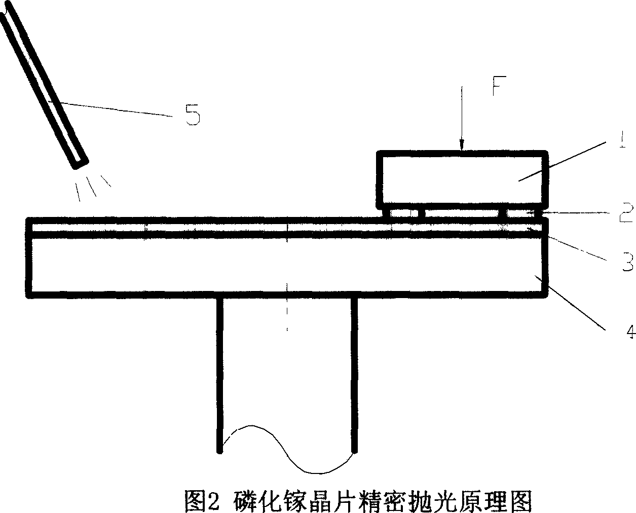
[0029] 5. On a precision surface grinding machine, use a gallium phosphide wafer nanoscale polishing solution composed of ammonium dichromate, polyoxyethylene amide, deionized water, etc. to perform global planar chemical mechanical polishing to obtain a gallium phosphide wafer nanoscale Surface roughness.

[0030] Gallium phosphide wafer polishing process parameters are:

[0031] Polishing disc speed: 70 rpm

[0032] Rotational spee...


PUM


Abstract

A nano-class super-smooth technology for processing the GaP wafer used to prepare blue and red LEDs includes such steps as adsorbing the GaP wafer on the bearing disc by water, plastic abrading, grinding, polishing and cleaning. Its dedicated grinding liquid, polishing liquid, cleaning liquid and their components are also disclosed.

Description

technical field [0001] The invention relates to an ultra-smooth surface processing technology of a gallium phosphide wafer used in the field of optoelectronics and optics. Background technique [0002] Gallium phosphide (GaP) crystal is an important basic material of modern industry, and has been widely used in optoelectronics, microelectronics, laser and other fields. The gallium phosphide wafers currently in use generally have the following problems: 1. The processing technology of the gallium phosphide wafer is complicated, and it needs to go through multiple grinding and polishing processes; 2. The roughness of the polished surface is relatively large, with Ra reaching 5 nanometers; the warpage is relatively large, 3. There is a processing strain layer on the surface of the gallium phosphide wafer. [0003] Poor quality gallium phosphide wafers make red and green light emitting diodes (LEDs) with poor luminous performance. Contents of the invention [0004] In order ...

Claims


Application Information

Patent Timeline
Patent Type & Authority Applications(China)
IPC IPC(8): B24B37/04H01L21/304
Inventor 周海
Owner 周海
Why Eureka
Try Eureka