Aligning system of photoetching apparatus and steping combined system of said aligning system thereof

An alignment system and lithography technology, applied in the field of level bonding systems, can solve problems such as affecting alignment accuracy, reducing diffraction efficiency, and quasi-signal strength attenuation, improving alignment accuracy, eliminating crosstalk effects, and difficulty in assembly and adjustment. little effect

Active Publication Date: 2007-04-18
SHANGHAI MICRO ELECTRONICS EQUIP (GRP) CO LTD
View PDF0 Cites 50 Cited by
  • Summary
  • Abstract
  • Description
  • Claims
  • Application Information

AI Technical Summary

Problems solved by technology

The system uses a single blazed grating optimized at the center wavelength to separate polychromatic light, which will reduce the diffraction efficiency of other color lights at the edge wavelength, resulting in attenuation of alignment signal strength and affecting alignment accuracy

Method used


Image

  • Aligning system of photoetching apparatus and steping combined system of said aligning system thereof
  • Aligning system of photoetching apparatus and steping combined system of said aligning system thereof
  • Aligning system of photoetching apparatus and steping combined system of said aligning system thereof

Examples


Embodiment Construction

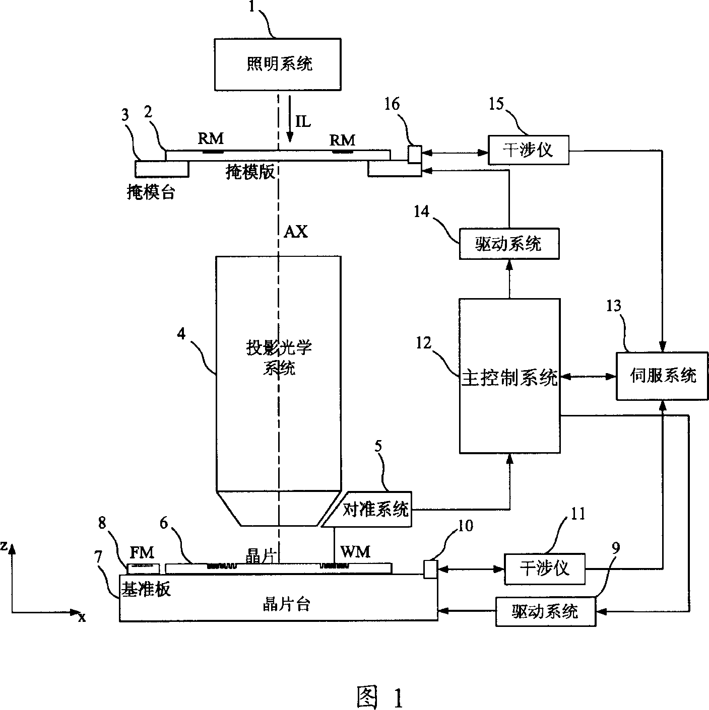
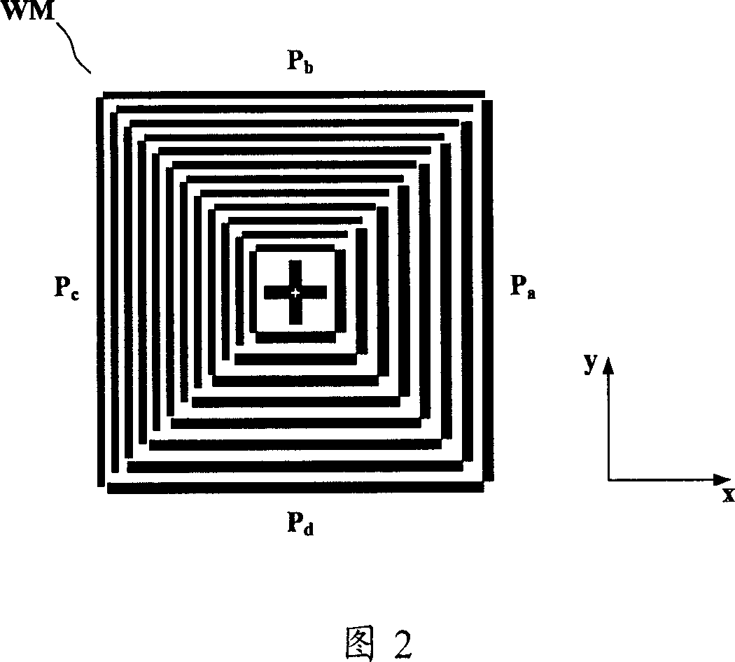
[0065] FIG. 1 is a schematic diagram of the overall layout and working principle of the alignment system of the lithography apparatus of the present invention and the level combination system of the alignment system and the existing lithography apparatus. As shown in Figure 1, the composition of the lithography apparatus includes: an illumination system 1 for providing an exposure beam; a mask holder and a mask table 3 for supporting a reticle 2, and the reticle 2 has a mask pattern and a periodic The alignment mark RM of the permanent structure; the projection optical system 4 for projecting the mask pattern on the reticle 2 onto the wafer 6; the wafer holder and the wafer stage 7 for supporting the wafer 6, and the wafer stage 7 is engraved with fiducials Reference plate 8 marked FM, alignment marks WM with periodic optical structures on wafer 6; alignment system 5 with stage bonding system and polychromatic light separation system for mask and wafer alignment; for mask table...


PUM


Abstract

The invention discloses mask-alignment aligning system and its grade combining system. The aligning system includes light source module, illumination module, imaging module, and detecting module. The grade combining system makes positive negative grade frequency spectrum facula of the alignment mark diffraction spectrum process corresponding overlap coherent, uses polychromatic light separating system to separate multiple wavelength light signal, measures light intensity or phase change at the corresponding position of the multiple wavelength multistage secondary diffracted facula to gain alignment mark position information. The invention has high alignment precision and stability.

Description

technical field [0001] The invention relates to a lithographic device in the field of integrated circuit IC or other micro device manufacturing, and in particular to an alignment system of the lithographic device and a level combination system of the alignment system. Background technique [0002] The photolithography apparatus in the prior art is mainly used in the manufacture of integrated circuits (ICs) or other micro devices. With a photolithographic apparatus, multilayer masks with different mask patterns are sequentially imaged in precise alignment on a photoresist-coated wafer, such as a semiconductor wafer or an LCD panel. Lithography devices are generally divided into two categories, one is a stepping lithography device, the mask pattern is exposed and imaged on one exposure area of ​​the wafer, and then the wafer moves relative to the mask to move the next exposure area to the mask pattern and under the projection objective, the mask pattern is again exposed on an...

Claims


Application Information

Patent Timeline
Patent Type & Authority Applications(China)
IPC IPC(8): G03F9/02G03F9/00G03F7/20
CPCG03F9/7049G03F9/7088
Inventor 徐荣伟李铁军李仲禹
Owner SHANGHAI MICRO ELECTRONICS EQUIP (GRP) CO LTD
Why Eureka
Try Eureka