An organic field effect transistor and its manufacture method

A technology of transistors and organic fields, applied in the field of organic field effect transistors and their preparation, can solve the problems that the size and position of dispersed crystals cannot be artificially controlled, the mechanical properties of organic crystals are poor, and the use of ultrasonic dispersion is limited, so as to avoid damage and simple equipment , to avoid the effects of radiation and damage

Inactive Publication Date: 2007-04-25
INST OF CHEM CHINESE ACAD OF SCI
View PDF0 Cites 17 Cited by
  • Summary
  • Abstract
  • Description
  • Claims
  • Application Information

AI Technical Summary

Problems solved by technology

However, the mechanical properties of organic crystals are generally poor, and they are easily broken and damaged during ultrasonic dispersion, which limits the use of ultrasonic dispersion
Moreover, the method of ultrasonic dispersion has great randomness, and the size and position of dispersed crystals cannot be artificially controlled.

Method used


Image

  • An organic field effect transistor and its manufacture method
  • An organic field effect transistor and its manufacture method

Examples


Embodiment 1

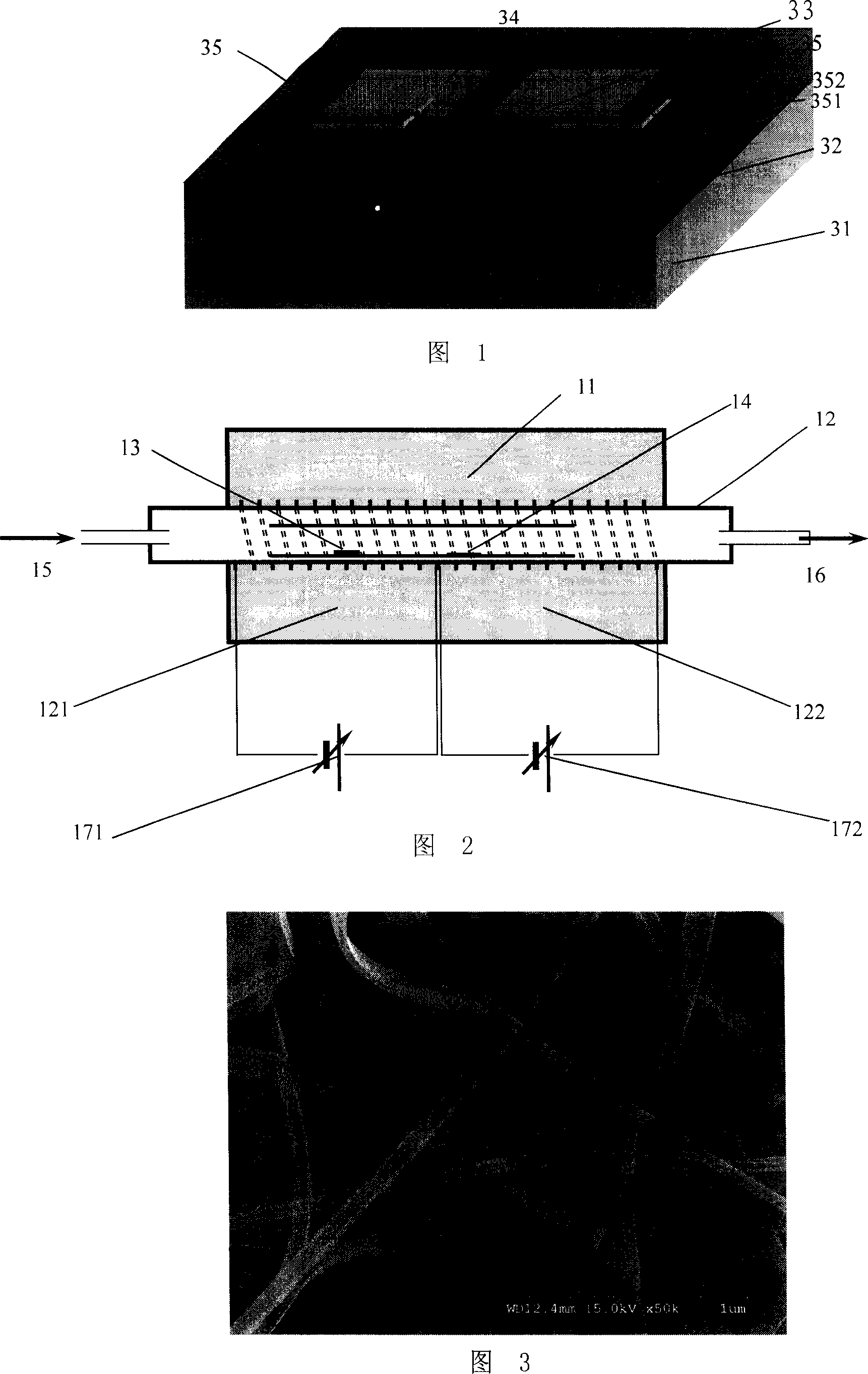
[0027] The structural representation of the field effect transistor of the present invention is as shown in Figure 1: two electrodes 35 (made up of a titanium layer 351 with a thickness of 5 nanometers and a gold layer 352 with a thickness of 70 nanometers) are laid on a substrate 31 with an insulating layer 32 in advance Above, these two electrodes serve as the source and drain of the transistor respectively, and the substrate 31 is also the gate of the transistor; the organic semiconductor single crystal micro / nano material 33 is located between the two electrodes 35, and its two ends pass through two metal films 34 are connected to two electrodes respectively, and the distance between the two metal layers can be adjusted to an appropriate level; according to the requirements of the device, the two metal layers can choose the same or different metal elements, only need to ensure that the metal film and the organic semiconductor It only needs to form ohmic contact between the ...


PUM


Abstract

The invention relates to an organic field-effect transistor, and relative production. Wherein, said transistor comprises a base plate as grid, an insulated layer on the base plate, a source grid and a leak electrodes on the insulated layer; there is an organic semi-conductor single-crystal micrometer/nanometer material between source and leak electrodes, whose two ends are connected to source and leak electrodes via two distanced metal films; the distance between two metal films is 5-20micrometer. The inventive transistor has high transfer rate and lower threshold voltage. And its production has following advantages that (1), it avoid organic solvent while will damage the nanometer material; (2), it has simple device to avoid radiating and damaging nanometer line by high-energy particles; (3), it can obtain controllable device; (4), it can control the structure of transistor, with better electrode contact.

Description

technical field [0001] The invention relates to an organic field effect transistor and a preparation method thereof. Background technique [0002] Organic field-effect transistors have attracted attention in recent years due to their potential applications in organic / molecular electronics. Organic field-effect transistors mainly include organic semiconductor conductive layers, insulating layers, and source, drain, and gate electrodes. Most of them use organic thin films as the conductive layer. Due to the presence of lattice disorder and grain boundary defects in thin films, the intrinsic properties of organic semiconductors are often masked, and the improvement of device mobility is also limited, and the higher defect concentration in thin films greatly increases the threshold of organic field effect transistors. Voltage. Low mobility and high threshold voltage overshadow the advantages of organic field-effect transistors while limiting their application in circuits. Due...

Claims


Application Information

Patent Timeline
Patent Type & Authority Applications(China)
IPC IPC(8): H01L51/05H01L51/10H01L51/40
Inventor 胡文平李洪祥汤庆鑫
Owner INST OF CHEM CHINESE ACAD OF SCI
Why Eureka
Try Eureka