An erasable metal-insulator-silicon capacitor structure with high density

A silicon capacitor and insulator technology, applied in the field of capacitors, can solve problems such as reducing device erasing efficiency, achieve fast programming/erasing characteristics, large storage window, and improve storage characteristics.

A silicon capacitor and insulator technology, applied in the field of capacitors, can solve problems such as reducing device erasing efficiency, achieve fast programming/erasing characteristics, large storage window, and improve storage characteristics.

CN1964075AInactive Publication Date: 2007-05-16FUDAN UNIV

Image

  • An erasable metal-insulator-silicon capacitor structure with high density
  • An erasable metal-insulator-silicon capacitor structure with high density
  • An erasable metal-insulator-silicon capacitor structure with high density

Examples


Embodiment Construction

[0023] The present invention is further specifically described below by way of examples.

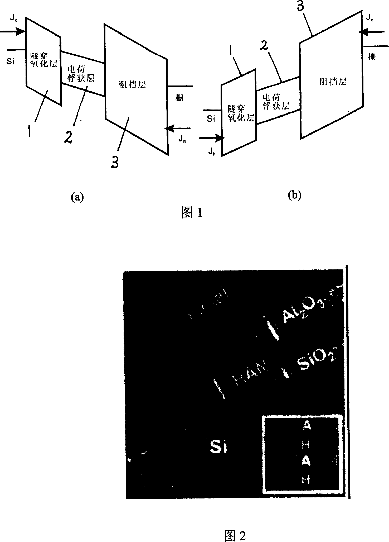
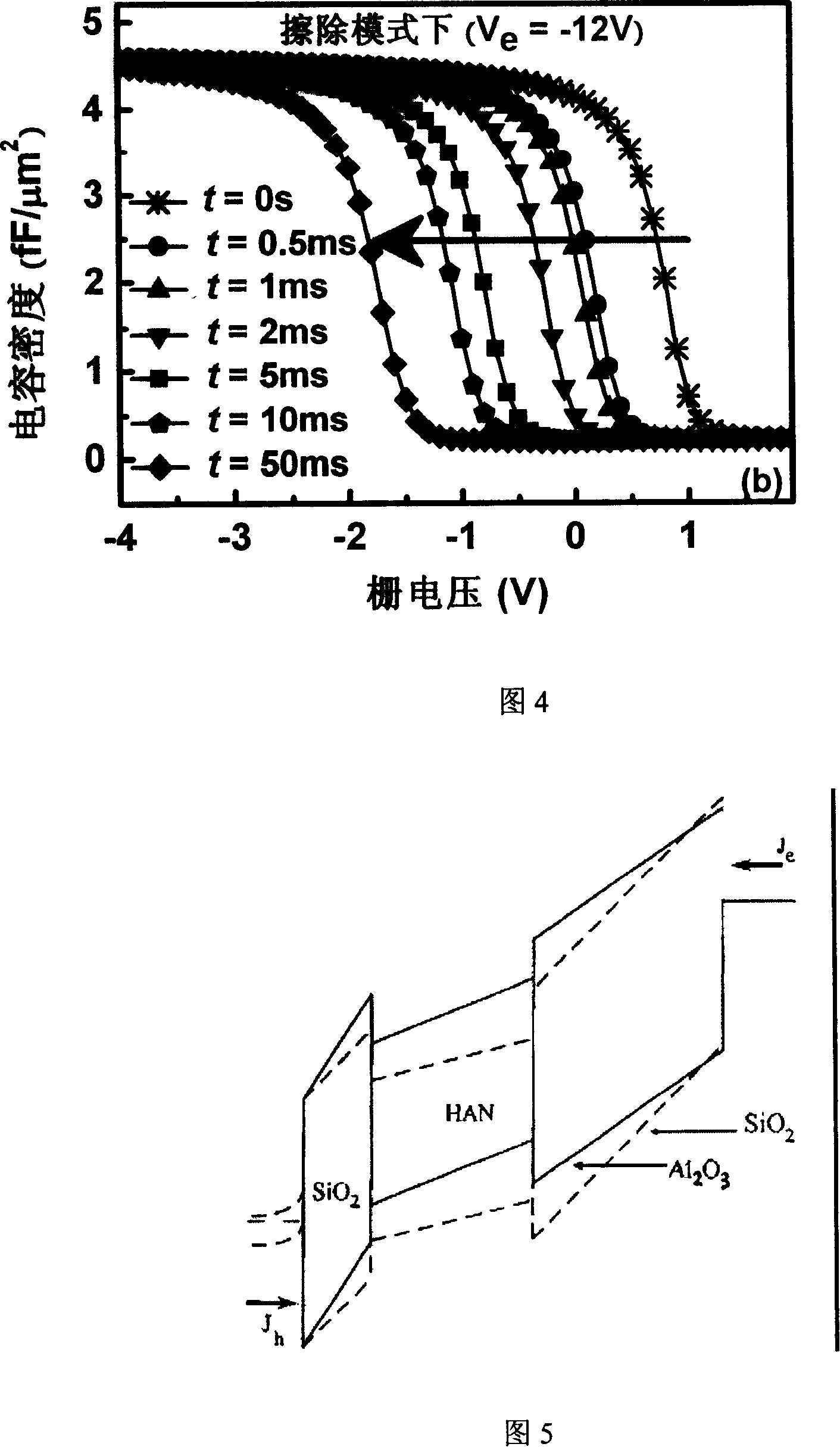
[0024] Using thermally oxidized SiO 2 Make a tunneling oxide layer with a physical thickness of 2-4 nanometers; then use HfO 2 / Al 2 o 3 The nano-laminated dielectric composed of the charge trapping layer, in which HfO 2 The physical thickness of the monolayer is 1-4 nm, Al 2 o 3 The physical thickness of a single layer is 0.5-2 nanometers, and the physical thickness of the entire HAN layer is 3-10 nanometers; with Al 2 o 3 As a barrier layer, its physical thickness is controlled at 6-12 nanometers. Finally, magnetron sputtered HfN or TaN is used as the metal gate. For example, on a 4-8Ωcm(100) p-type Si substrate, a layer of 2.7nm SiO is grown by thermal oxidation first. 2 , and then alternately grow 2nm HfO by atomic layer deposition (ALD) 2 , 1nm Al 2 o 3 The resulting HAN charge-trapping layer has a total physical thickness of 6 nm. Next, a layer of 8nm Al was deposited ...


PUM

PropertyMeasurementUnit
Thicknessaaaaaaaaaa
Thicknessaaaaaaaaaa
Thicknessaaaaaaaaaa

Abstract

The related PE-MIS capacitor employs SiO2 / HfO2-Al2O3 nano (HAN) / Al2O3 medium structure, and has capacitance density up to 4.5fF / mum2, storage window up to 1.45V when programming at 12V voltage and erasing for 5ms at -12V voltage. This invention increases voltage drop on SiO2 layer, and thereby prevent Fowler-Nordheim tunneling current efficiently.

Description

technical field [0001] The invention belongs to the technical field of capacitors, in particular to a high-density rewritable metal-insulator-silicon capacitor structure. Background technique [0002] The growing market of portable electronic products has greatly stimulated the research and development of non-volatile memory. Among many non-volatile storage structures, flash memory is the best due to its excellent performance and good process compatibility 1 . In recent years, due to the continuous shrinking of memory cells, the next-generation flash memory based on silicon dioxide / silicon nitride / silicon dioxide (ONO) dielectric structure has received extensive attention and research 1-4 , because the polysilicon / ONO / silicon (SONOS) structure has lower cost and radiation resistance characteristics. In the usual SONOS structure, silicon nitride is used as the charge storage layer, and silicon dioxide is used as the blocking oxide layer. However, erase saturation and low c...

Claims


Application Information

Patent Timeline
16 May 2007
Publication
CN1964075A
IPC
H01L29/792; H01L29/51; H01L27/115
Inventors
丁士进; 陈玮