Semiconductor device
一种半导体、天线的技术,应用在半导体器件、半导体/固态器件零部件、电固体器件等方向,能够解决产率降低、增加布线连接工序等问题,达到提高产率、防止劣化的效果
- Summary
- Abstract
- Description
- Claims
- Application Information
AI Technical Summary
Problems solved by technology
Method used
Image

Examples
Embodiment approach 1
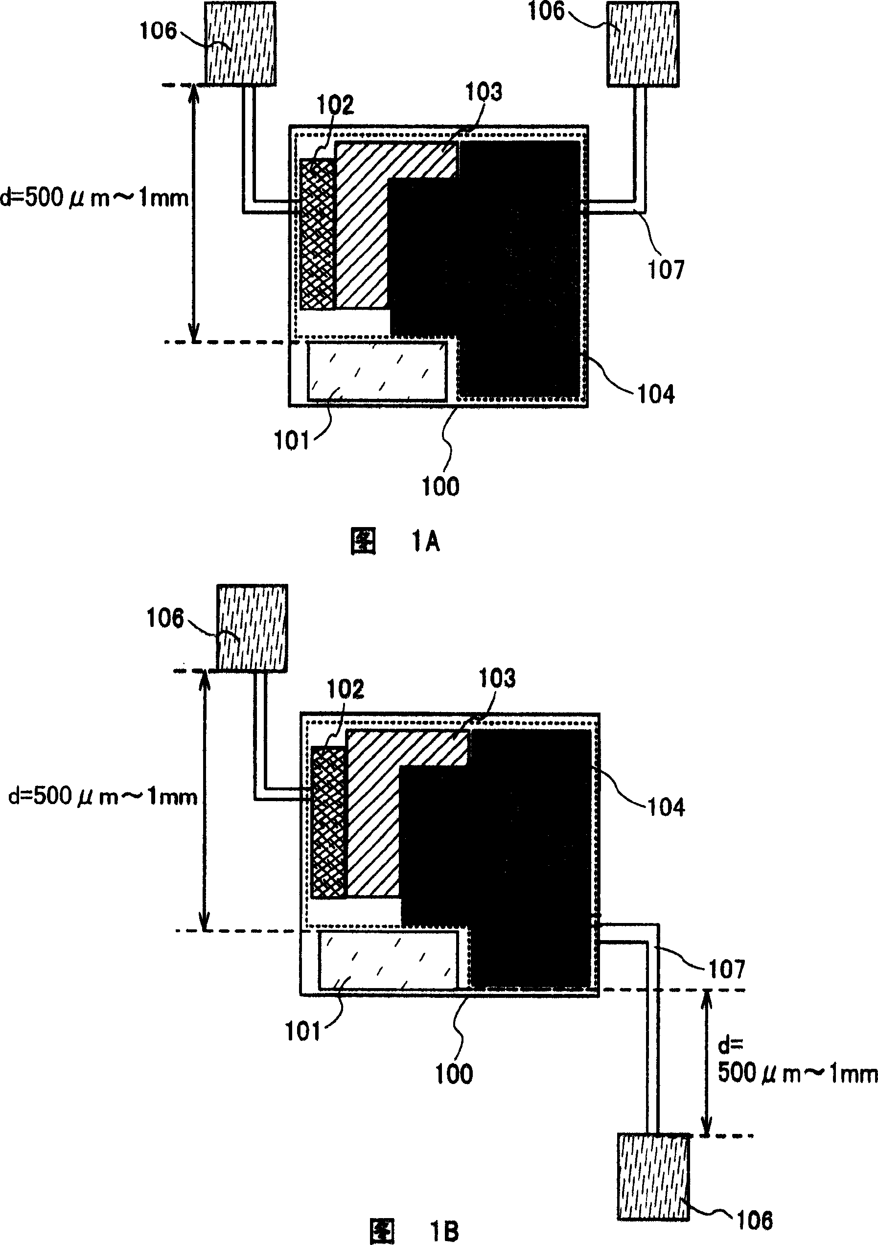
[0052] In this embodiment mode, the configuration of a wireless chip having an organic memory will be described. In addition, although the present embodiment only describes the configuration of a wireless chip, wireless communication can be performed by providing antennas on it according to the communication frequency.
[0053] 1A shows a wireless chip 100, in which a storage area 101, a high-frequency circuit unit including an external signal input unit 102 and an RF input unit 103, and a logic circuit unit 104 are provided, and pads 106 are provided on the outside.
[0054] The storage area 101 is an area in which information is written, and is provided with ROM or RAM. In this embodiment, the unique information of the wireless chip is written in the ROM. The ROM cannot be rewritten, that is, the so-called write-once type. Therefore, information that does not need to be rewritten or information that should not be rewritten such as inherent information of the wireless chip ...
Embodiment approach 2
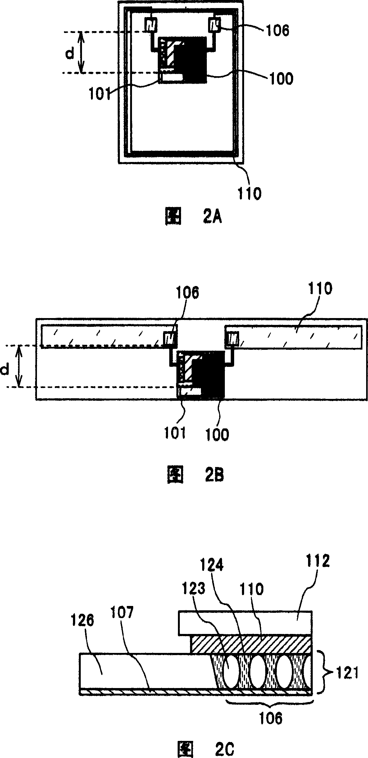
[0063] In this embodiment, a form of a wireless chip including an antenna will be described.
[0064] FIG. 2A shows a method in which an antenna 110 having a coil shape is connected to the wireless chip 100 via pads 106 corresponding to the data transfer method of the electromagnetic induction method. The advantage of the electromagnetic induction method is that the directivity of the antenna is wide and the communication range is large. As the frequency band, a long-wave band such as 135 kHz and a short-wave band such as 13.56 MHz are used. The communication distance is several centimeters to tens of centimeters. The distance between pad 106 and memory region 101 is 500 μm or more, preferably 750 μm or more, expressed in a range of 500 μm to 1 mm inclusive.
[0065] By employing such a structure, it is possible to prevent damage or deformation of the wireless chip, particularly, the memory region when the antenna is bonded under pressure.
[0066] FIG. 2B shows how the dip...
Embodiment approach 3
[0071] In this embodiment, an example of a mask layout of a wireless chip will be described.
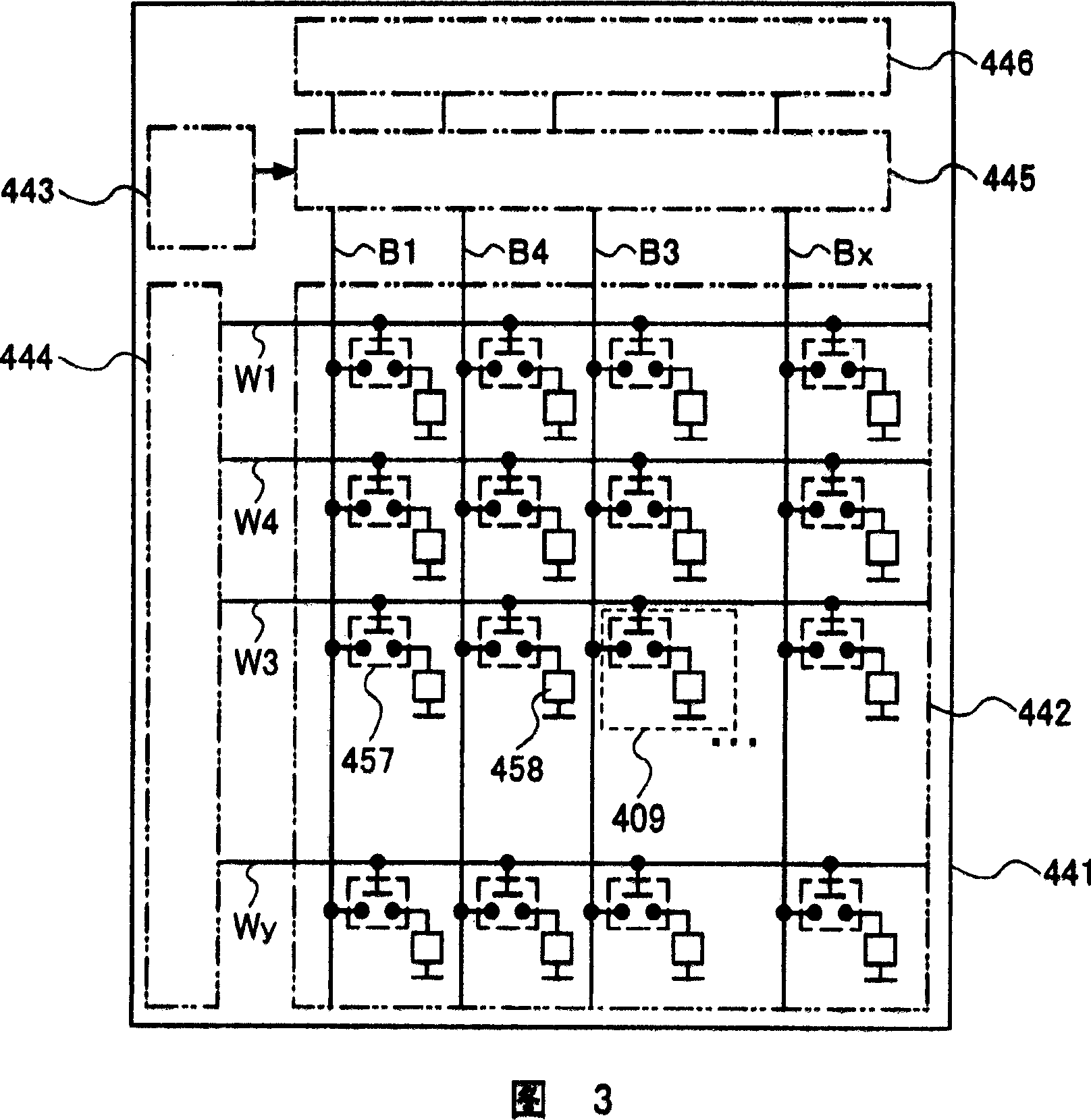
[0072] FIG. 11A shows an example of a mask layout of a wireless chip, and FIG. 11B shows a block diagram thereof.
[0073] In the wireless chip, a logic circuit unit 402 occupying the largest area, an RF input unit 401 , and a storage area 404 next to it are provided. An adjustment circuit section 405 and a resistor 407 are provided in a partial area in the storage area 404 , and the adjustment circuit section 405 is provided beside the resistor 407 . The external signal input unit 403 is provided beside the RF input unit 401 . Since the external signal input unit 403 has pads, it is preferably provided in a region in contact with one side of the wireless chip 100 . This is because it is possible to bond with one side of the wireless chip as a reference when connecting the pads.
[0074] At this time, the distance between the pad and the storage region is 500 μm or more, preferabl...
PUM
 Abstract
Description
Claims
Application Information
 - R&D
- Intellectual Property
- Life Sciences
- Materials
- Tech Scout
- Unparalleled Data Quality
- Higher Quality Content
- 60% Fewer Hallucinations
Browse by: Latest US Patents, China's latest patents, Technical Efficacy Thesaurus, Application Domain, Technology Topic, Popular Technical Reports.
© 2025 PatSnap. All rights reserved.Legal|Privacy policy|Modern Slavery Act Transparency Statement|Sitemap|About US| Contact US: help@patsnap.com