Method for manufacturing multilayer wiring substrate with cable

A manufacturing method and a technology of a flexible wiring substrate, applied in multilayer circuit manufacturing, printed circuit manufacturing, electrical components, etc., can solve the problems of reducing wiring density, difficulty in forming micro-circuits, increasing wiring layers, etc., to ensure reliability and productivity Good, high pass rate effect

Inactive Publication Date: 2007-05-30
NIPPON MEKTRON LTD
View PDF3 Cites 14 Cited by
  • Summary
  • Abstract
  • Description
  • Claims
  • Application Information

AI Technical Summary

Problems solved by technology

[0049] As described above, as a problem when using the conventional manufacturing method to manufacture a multilayer wiring board having an improved integration level and a cable portion capable of mounting narrow-pitch CSPs, since complex punching and plating are required many times, there is a problem in terms of productivity and There is a problem in the pass rate, the number of wiring layers to be thickened by plating increases, and it is difficult to form a fine circuit, so multi-stage combination may not be able to reduce the wiring density

Method used


Image

  • Method for manufacturing multilayer wiring substrate with cable
  • Method for manufacturing multilayer wiring substrate with cable
  • Method for manufacturing multilayer wiring substrate with cable

Examples


Embodiment approach 1

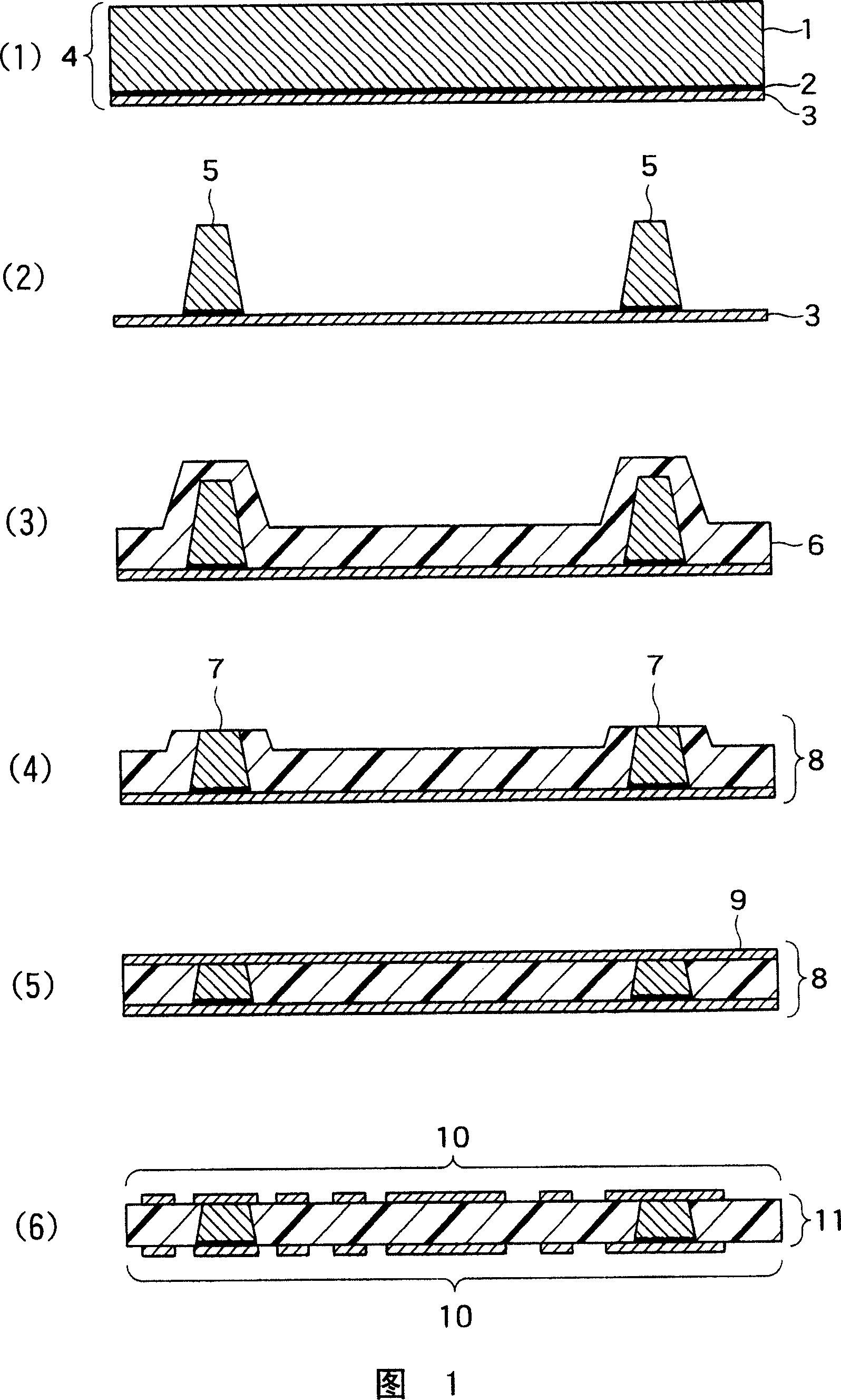
[0091] 1 to 5 are cross-sectional process diagrams showing Embodiment 1 of the present invention. First, as shown in FIG. 2 (for example, thickness 2 μm) / copper foil 3 (for example, thickness 12 μm) three-layer metal substrate 4 .

[0092] Next, as shown in FIG. 1(2), conductive protrusions 5 are formed on the copper foil 3 by selective etching. The etching solution at this time uses an etching solution used in a conventional copper etching process, such as an etching solution containing copper chloride, to etch about 80 to 90% of the overall thickness of the copper foil 1; An etchant for selectively etching copper, such as an alkaline etchant containing ammonia, etch and remove the remaining portion of the copper foil 1 to expose the nickel foil; Hydrogen oxide or nitric acid etchant is used to etch and remove the exposed nickel foil 2 . Thus, the structure shown in Fig. 1(2) is obtained.

[0093] Next, as shown in FIG. 1 (3), the preform 6 in the state of section B is pas...

Embodiment approach 2

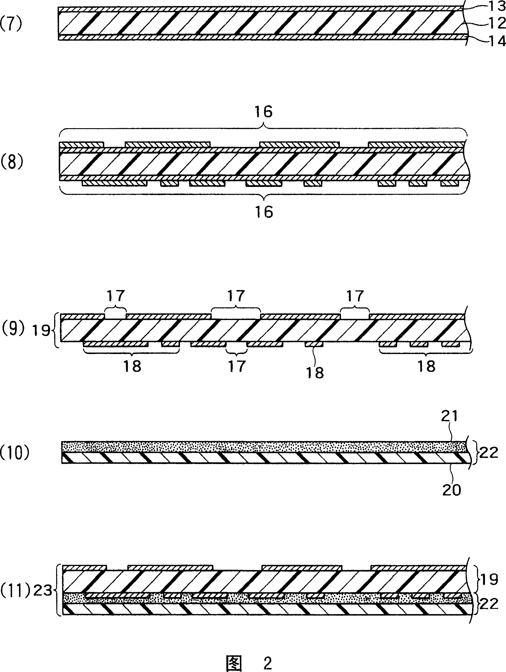
[0119] 6 to 9 are cross-sectional process diagrams showing Embodiment 2 of the present invention. First, as shown in FIG. 6(1), when manufacturing a double-sided flexible wiring board, prepare a Metal substrate 54 having a three-layer structure of nickel foil 2 (for example, thickness 2 μm) / copper foil 53 (for example, thickness 12 μm).

[0120] Next, as shown in FIG. 6(2), conductive protrusions 55 are formed on the copper foil 53 by selective etching. The etching solution at this moment, at first, uses the etching solution that adopts in conventional copper etching process, for example the etching solution containing cupric chloride etches about 80~90% of the overall thickness of copper foil 1; , an etchant that selectively etches copper, for example an alkaline etchant containing ammonia to etch away the remaining portion of the copper foil 1 to expose the nickel foil; then, use an etchant that is less corrosive to copper and selectively etches nickel, for example containin...


PUM


Abstract

The invention provides a method for inexpensively and stably manufacturing a multilayer wiring board having a cable section with a high integration degree capable of loading narrow pitch CSP. The manufacturing method of the multilayer flexible wiring board having the cable section in at least an outer layer, includes a) a process for manufacturing an inner layer core substrate (8, 58); b) a process for forming an opening of copper foil in a conduction hole forming part on an outer layer side in a double sided copper clad laminate having flexibility, and forming a circuit pattern (10, 60) comprising an opening of a conduction hole forming part on an inner layer side of the double sided copper clad laminate; c) a process for forming a cover ray (22, 70) on the circuit pattern to make it to be an outer layer built-up layer (23, 67); d) a process for laminating the outer layer built-up layer by turning a side where the cover ray is formed to a side of the inner layer core substrate, and forming the lamination circuit substrate (25, 73); e) a process for performing laser processing on the conduction hole forming part of the outer layer side through the opening of copper foil, and forming a conduction hole (26, 27, 28, 74, 75, 76) in the lamination circuit substrate; f) a process for performing laser processing on the conduction hole forming part of the outer layer side by acting the opening of the copper foil and the opening of the conduction hole forming part as a mask for shielding laser, and forming the conduction hole in the lamination circuit substrate; and g) a process for performing a conduction processing on the conduction hole, and forming a via hole (29, 30, 31, 77, 78, 79) with electrolytic plating. The double sided copper clad laminate can be replaced by a single sided copper clad laminate.

Description

technical field [0001] The present invention relates to a manufacturing method of a composite multilayer wiring substrate, in particular to a manufacturing method of a composite multilayer flexible wiring substrate having a flexible cable portion. Background technique [0002] In recent years, miniaturization and higher functionality of electronic devices have been increasingly advanced, and for this reason, there has been an increased demand for higher densities of wiring boards. Therefore, by changing the wiring board from one side to a multilayer wiring board having two sides or three or more layers, the density of the wiring board can be increased. [0003] As this link, centering on small electronic devices such as mobile phones, there are separate flexible wiring boards or flat flexible cables that are connected through connectors or the like between multilayer wiring boards or hard wiring boards on which various electronic components are mounted. A multilayer flexibl...

Claims


Application Information

Patent Timeline
Patent Type & Authority Applications(China)
IPC IPC(8): H05K3/46H05K3/42
CPCH05K1/0393H05K3/429H05K3/4623
Inventor 松田文彦
Owner NIPPON MEKTRON LTD
Why Eureka
Try Eureka