Method for deeply etching one-dimensional photon crystal based on focusing ion
A technology for one-dimensional photonic crystals and focused ion beams, which is applied in the field of realizing submicron-scale high-aspect-ratio periodic groove structure gratings and periodic one-dimensional photonic crystals. Long cycle and other issues
- Summary
- Abstract
- Description
- Claims
- Application Information
AI Technical Summary
Problems solved by technology
Method used
Image

Examples
Embodiment Construction
[0023] The preferred embodiment of the present invention is described in more detail below with reference to the accompanying drawings of the present invention.
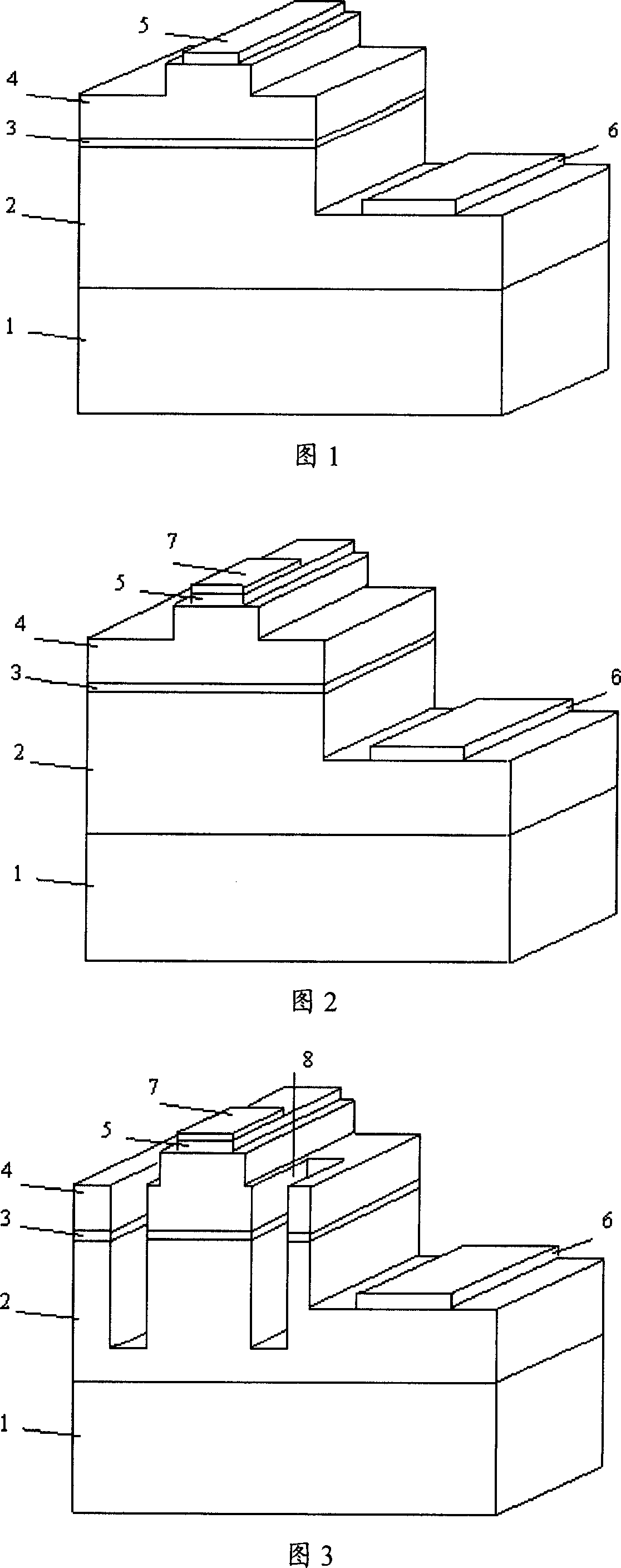
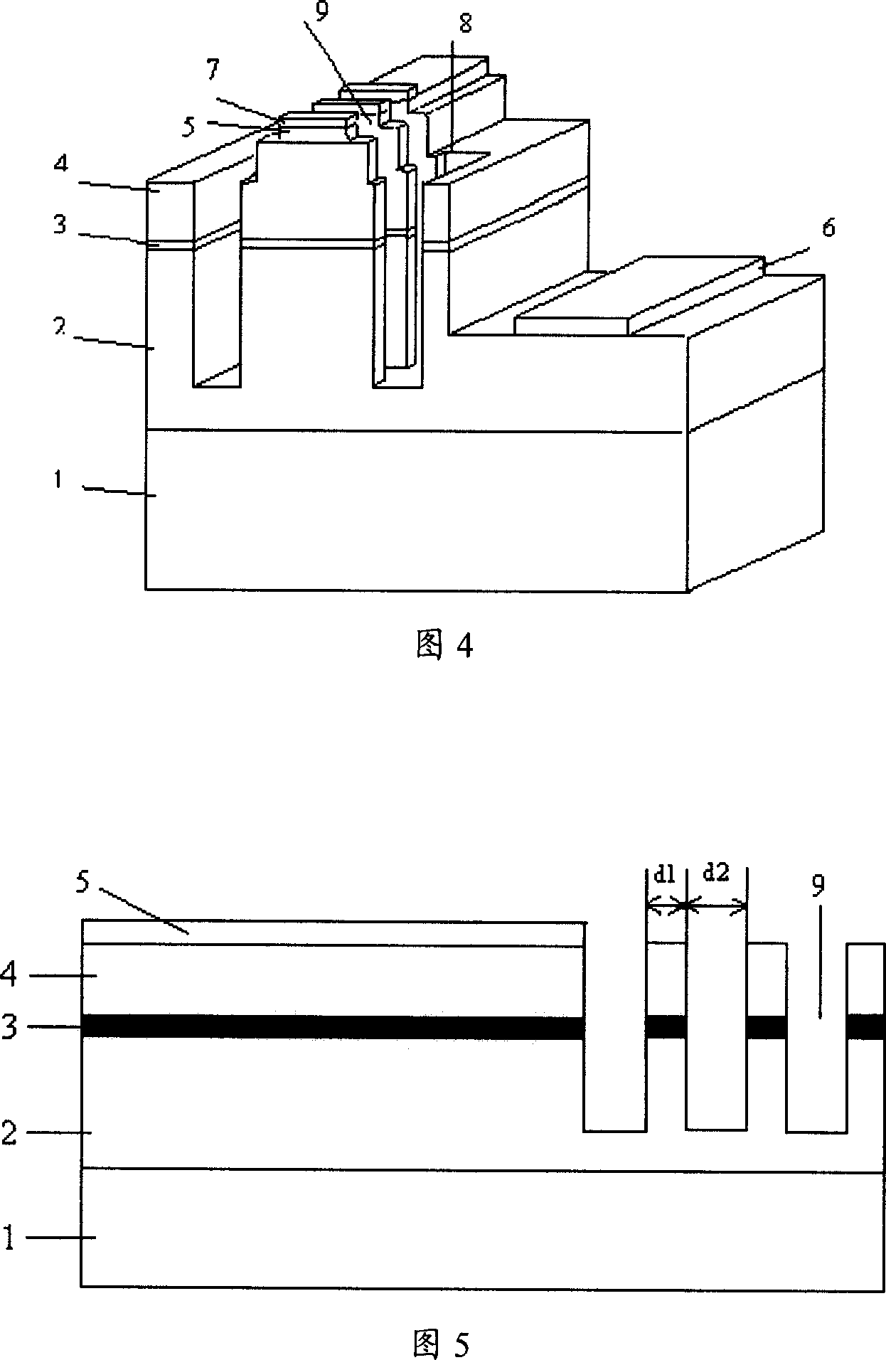
[0024] In this embodiment, the GaN laser with a center wavelength of 405nm is used as the processing object, and the one-dimensional photonic crystal reflective mirror surface is fabricated by FIB technology as the best example to illustrate the present invention.
[0025] The nitride-based laser diode structure used in the example is a typical edge-emitting semiconductor laser structure, as shown in Figure 1, it is worth pointing out that the structure of Figure 1 can also be replaced by semiconductor samples of other structures, that is, using the present invention to focus ion Beam etching technology also realizes deeply etched one-dimensional photonic crystals on other semiconductor samples. The epitaxial multilayer structure of the semiconductor laser diode core is a traditional "separately confinement" structur...
PUM
 Abstract
Description
Claims
Application Information
 - R&D
- Intellectual Property
- Life Sciences
- Materials
- Tech Scout
- Unparalleled Data Quality
- Higher Quality Content
- 60% Fewer Hallucinations
Browse by: Latest US Patents, China's latest patents, Technical Efficacy Thesaurus, Application Domain, Technology Topic, Popular Technical Reports.
© 2025 PatSnap. All rights reserved.Legal|Privacy policy|Modern Slavery Act Transparency Statement|Sitemap|About US| Contact US: help@patsnap.com