Method of manufacturing a complementary metal oxide silicon image sensor

A technology of image sensor and manufacturing method, applied in semiconductor/solid-state device manufacturing, electric solid-state device, semiconductor device, etc., can solve problems such as uncleanness, rough surface of pad, residual circular defect, etc.

Inactive Publication Date: 2007-07-04
DONGBU ELECTRONICS CO LTD
View PDF0 Cites 3 Cited by
  • Summary
  • Abstract
  • Description
  • Claims
  • Application Information

AI Technical Summary

Problems solved by technology

Although the scrubbing and cleaning process was performed to remove the circular defect 145 prior to the cleaning and pad treatment process, the circular defect 145 still re

Method used


Image

  • Method of manufacturing a complementary metal oxide silicon image sensor
  • Method of manufacturing a complementary metal oxide silicon image sensor
  • Method of manufacturing a complementary metal oxide silicon image sensor

Examples


Embodiment Construction

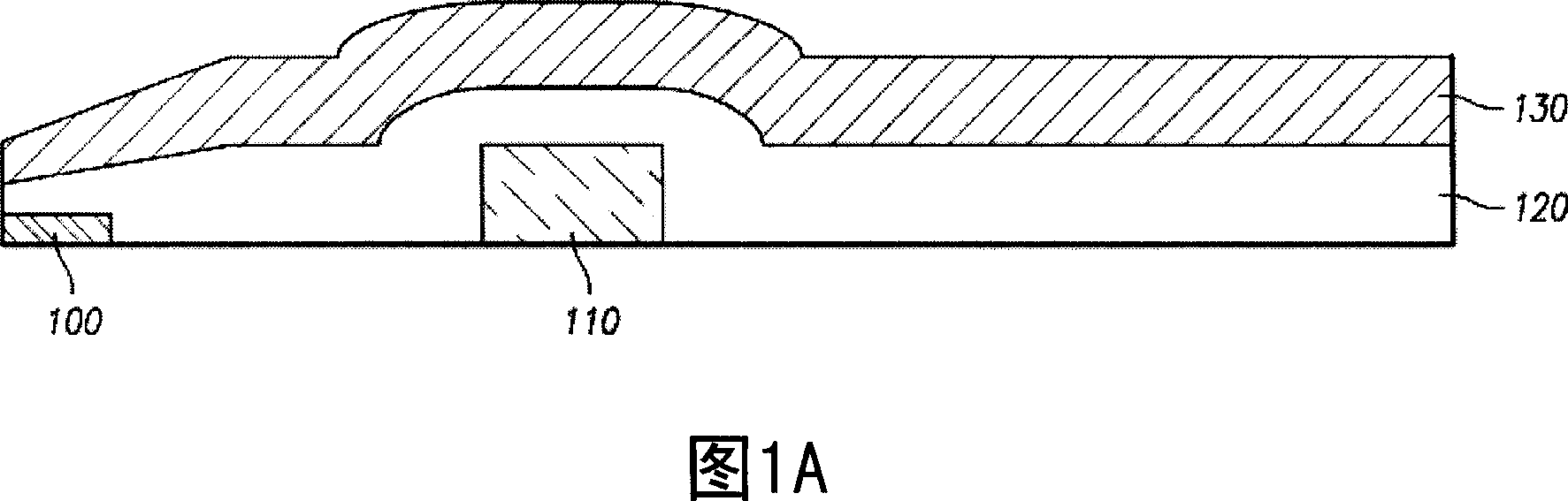
[0012] A preferred embodiment of the present invention is described below with reference to FIGS. 2A to 2D. 2A to 2D are cross-sectional views illustrating several processes after the pad 210 is formed.

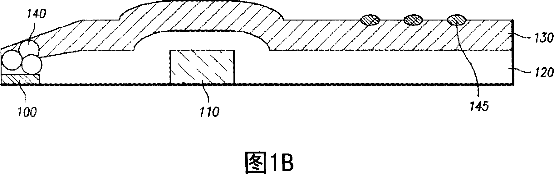
[0013] FIG. 2A shows a state where an oxide passivation layer 220 (hereinafter referred to as oxide layer 220 ) and a nitride passivation layer 230 (hereinafter referred to as nitride layer 230 ) have been formed after pad 210 is formed. Referring to FIG. 2A, after the oxide layer 220 is coated, a chemical mechanical polishing (CMP) process is performed, and then the nitride layer 230 is coated. In addition, since the edge of the wafer is processed several times by each light treatment, the irregular residual layer 100 is formed in the edge region of the wafer.

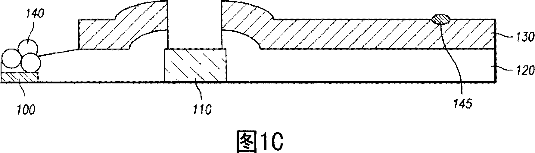
[0014] FIG. 2B shows a situation where the pad 210 is exposed through a photolithography process. In this case, the oxide layer 220 and the nitride layer 230 at the edge portion of the wafer are etched and removed....


PUM

PropertyMeasurementUnit
Thicknessaaaaaaaaaa

Abstract

The invention discloses a method for manufacturing a CMOS image sensor. The method includes following steps: depositing an oxide layer and a nitride layer over the substrate after forming a pad over a substrate; exposing and cleaning the pad by etching the oxide layer and the nitride layer; depositing a pad protection layer; performing a hydrogen anneal process; performing a micro-lens process, a planarization process, and a color filter array process; and removing the pad protection layer over a pad area. Thereby a shedding phenomenon and a circular fault of the nitride layer are prevented.

Description

technical field [0001] The present invention relates to a manufacturing method of a semiconductor device, more particularly, the present invention relates to a manufacturing method of a complementary metal-oxide-semiconductor (CMOS) image sensor, especially to a process after forming a pad on a metal interconnection layer. Background technique [0002] Unlike typical semiconductor manufacturing processes, in the case of CMOS image sensors, the hydrogen annealing (sintering) process for improving low-illumination characteristics is generally not performed after the stacked oxide passivation layer, but after the stacked nitride passivation layer Afterwards. This causes various problems related to the weak interlayer stress of the nitride layer in the edge region of the wafer. [0003] Problems of the prior art are described below with reference to FIGS. 1A-1I . 1A is a cross-sectional view illustrating a process of coating an oxide passivation layer 120 and a nitride passiva...

Claims


Application Information

Patent Timeline
IPC IPC(8): H01L21/82H01L27/146
CPCH01L27/14698H01L27/146
Inventor 金唇翰
Owner DONGBU ELECTRONICS CO LTD
Why Eureka
Try Eureka