Housing for an infrared radiation micro device and method for fabricating such housing

a micro-device and infrared radiation technology, applied in the field of infrared radiation micro-devices, can solve the problems of reducing the insertion loss of pre-fabricated micro-structured surface textures, negatively affecting the geometry of structure, and high insertion loss, so as to improve background detection and improve image quality. , the effect of high pass property

Active Publication Date: 2018-06-19
FRAUNHOFER GESELLSCHAFT ZUR FOERDERUNG DER ANGEWANDTEN FORSCHUNG EV +1
View PDF25 Cites 2 Cited by
  • Summary
  • Abstract
  • Description
  • Claims
  • Application Information

AI Technical Summary

Benefits of technology

[0026]The distance frame is made of silicon, preferably of poly-crystalline silicon at least in part. By the use of silicon for the distance frame, in the case of a silicon cover and/or a silicon substrate thermo mechanical stresses on the cover are reduced in comparison to thin film anti-reflective coating deposition. The additive deposition process of the distance frame structures with advantage is a mature process with sufficient wafer throughput. Preferably, the silicon distance frame is build around the antireflective surface texture. The cavity formed by the silicon distance frame preferably is about 1-1000 μm deep. The silicon distance frame preferably is 20 μm to 800 μm wide, most preferred 80-300 μm. Preferably, the silicon distance frame is substance-to-substance bonded to the cover and/or the substrate. This means that no additional adhesive, glasfrit or metal layer has to be used. Again preferred, between the silicon distance frame and the cover and the substrate, respectively, there is no silicon oxide layer.
[0027]The infrared micro unit may be an infrared sensor, an infrared micro-bolometer, an infrared micro-mirror or an infrared radiation emitting micro-device. Especially it may be a common micro-bolometer sensor array. It is arranged in the cavity defined by cover, substrate and distance frame, which is hermetically sealed against the environment. In the cavity a vacuum or at least a very low pressure atmosphere is provided. According to a preferred embodiment of the invention the infrared micro unit is arranged on the substrate, preferably opposite the antireflective surface texture of the cover.
[0028]Additional IR micro units, especially infrared sensor elements, can be positioned beside the IR micro unit of each device, especially beside an IR micro bolometer unit. The additional IR micro bolometer units are not necessarily exposed to 8 μm to 12 μm infrared radiation. These specific sensor elements enable device self test functionalities, such as cavity vacuum check, improved background detection and further functions.
[0029]According to a preferred embodiment of the invention a thin film antireflective coating is arranged on the substrate far side of the cover opposite of the antireflective surface texture on the substrate side of the cover. Preferably, the thin film antireflective coating has a high pass property for wavelengths longer than 5.5 or 8 μm. The thin film antireflective coating can act as a filter that eliminates such short wavelength and is advantageous for image quality due to fading out certain parts of sunlight for example. While it is of advantage to provide the antireflective surface texture on the substrate side of the cover i.e. on the side of the cover facing the cavity housing the infrared

Problems solved by technology

It is a drawback of this method that the etching process of the cavity after forming the surface texture negatively affects the geometry of the structure, especially the side geometry of the posts whose diameters are reduced and whose profiles become cone shaped if not the posts are transformed in flat lens shaped structures.
The loss of geometry and shape results in an undesirable higher reflection of the incoming IR-radiation and accordingly causes higher insertion losses.
The fabrication of a micro-structured surface texture with geometrical specifications capable of reducing insertions losses inside a pre-fabricated cavity deeper than 50 μm is challenging and is far beyond the state of the art.
The reason for this is that high resolution wafer steppers required to generate the fine details of the micro-structured surface texture for reducing the reflection losses of IR-radiation have a limited depths of focus, which makes their usage for the texturing process at the bottom of the

Method used


Image

  • Housing for an infrared radiation micro device and method for fabricating such housing
  • Housing for an infrared radiation micro device and method for fabricating such housing
  • Housing for an infrared radiation micro device and method for fabricating such housing

Examples


Embodiment Construction

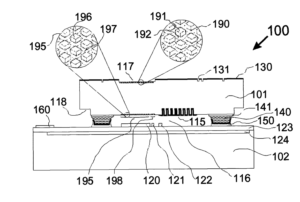
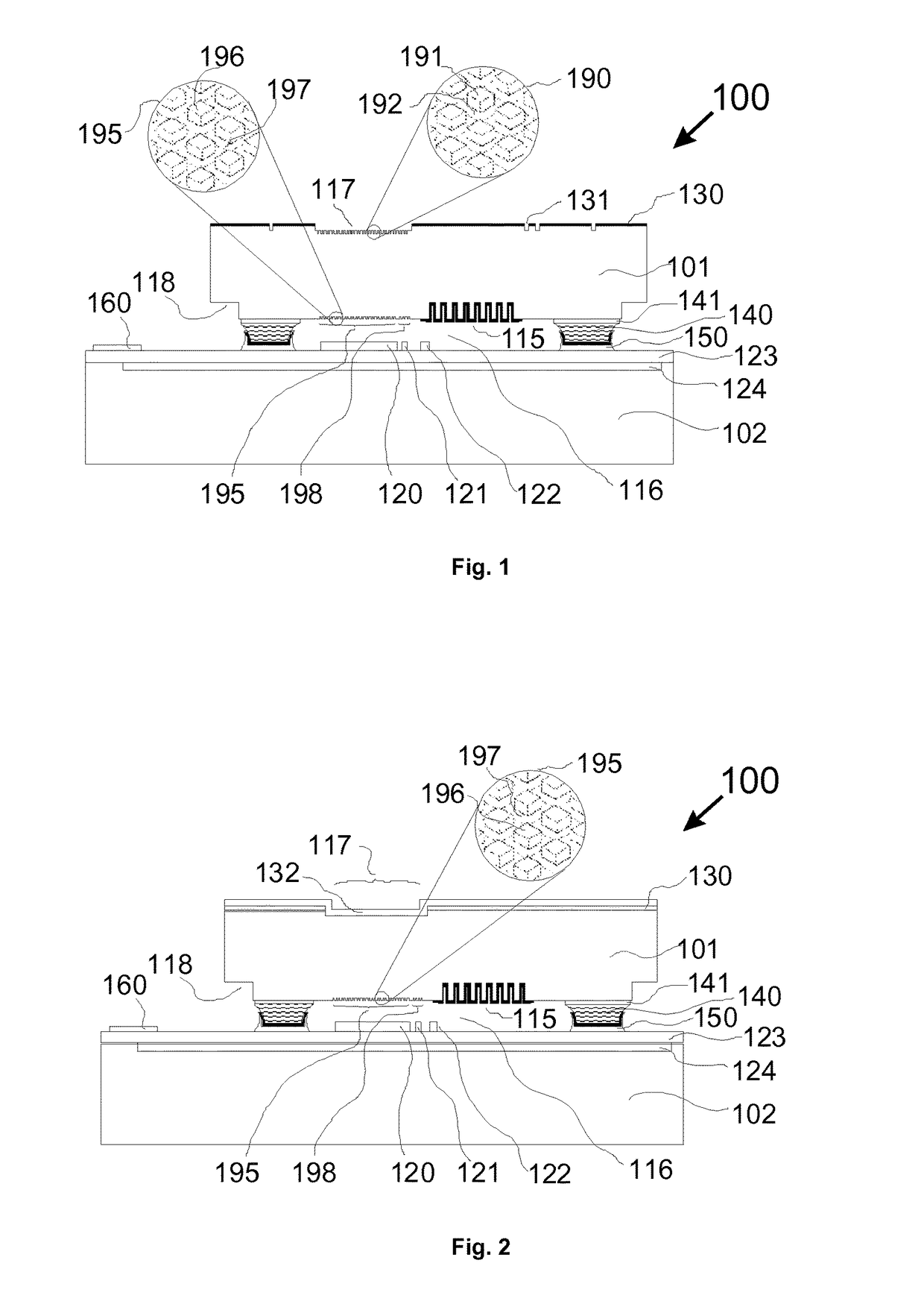
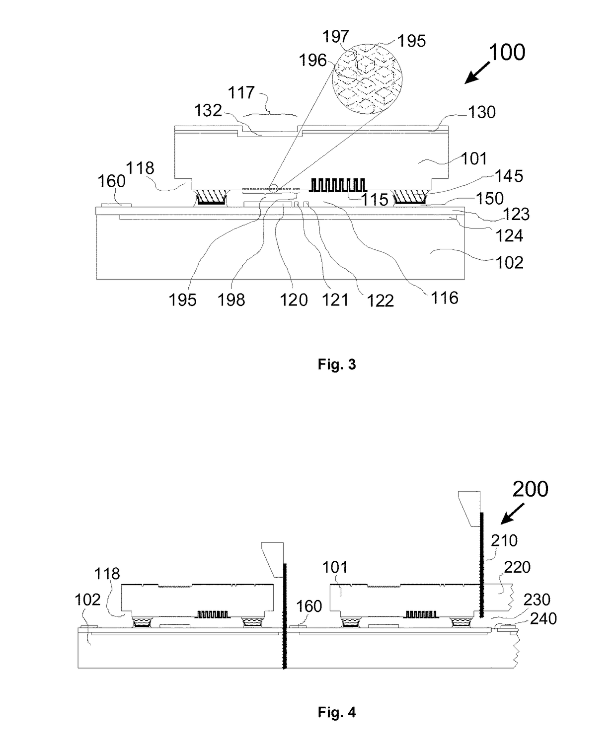
[0068]Reference is made to FIG. 1 showing an example of a infrared micro-bolometer array sensor 100 according to the invention. FIG. 1 shows the sensor 100 in a cross section of a representative package construction. Two round silicon wafers 101 and 102 with a diameter of 100 mm or larger and a thickness of not less than 300 μm are used; although other infrared transparent substrate materials such as germanium are suitable. A double side polished, high resistively silicon cover wafer with more than 1 Ohm·cm resistance, low crystal defect density and low oxygen content is preferred to fabricate the cover 101 to reduce the infrared absorption in the material of the cover 101.

[0069]A cavity 116 is formed by the use of a distance frame 140 arranged between cover 101 and substrate 102. The distance frame 140 encloses bolometer sensors 120, 121 and 122, which are examples for the IR-micro units, and a getter layer 115.

[0070]The distance frame 140 is made of silicon and has rounded side wa...


PUM


Abstract

Infrared radiation micro device, cover for such a device and method for its fabrication, the device comprising a substrate and a cover and an infrared radiation detecting, emitting or reflecting infrared micro unit, the infrared micro unit being arranged in a cavity defined between the substrate and the cover, the cover comprising an antireflective surface texture to enhance the transmissibility of infrared radiation, wherein a distance frame formed in an additive process on the substrate side of the cover and/or the cover side of the substrate is arranged between substrate and cover.

Description

BACKGROUND OF THE INVENTIONField of the Invention[0001]The application relates to the field of infrared radiation micro devices as for example infrared micro-bolometer sensors, infrared micro-mirrors or infrared radiation emitting micro-devices. The application also refers to the packaging and the method of production of such devices, especially on wafer level.Description of Related Art[0002]Uncooled infrared array detectors based on resistive bolometer micro-bridges integrated on CMOS read out circuits have shown their potential in a variety of applications working typically with wavelength in the range of about 8 μm to 14 μm. The detection principle of infrared radiation is based on the temperature rise of the micro-bolometer arrays acting as detector by absorbed IR-radiation causing a change of electrical resistance that is measured. The performance of uncooled micro-bolometer arrays on a semiconductor substrate depends greatly on their thermal isolation. Due to this, the bolomet...

Claims


Application Information

Patent Timeline
IPC IPC(8): H05K5/00C25D5/02H05K13/00H01L27/146G01J5/04G01J5/08
CPCH01L27/14618G01J5/045G01J5/0875H01L27/14683H01L2924/01327H01L2924/01322H01L2924/01079H01L2924/1461H01L2924/10158H01L2924/10157H01L27/14649H01L2224/16H01L2924/01019H01L2924/01057H01L2924/01077H01L2924/01078H01L2924/00H01L27/14605
Inventor REINERT, WOLFGANGQUENZER, JOCHENTINNES, SEBASTIENROMAN, CECILE
Owner FRAUNHOFER GESELLSCHAFT ZUR FOERDERUNG DER ANGEWANDTEN FORSCHUNG EV
Why Eureka
Try Eureka