

Adhesive agent composition for multilayer semiconductor
a technology of adhesive agent and semiconductor, applied in the direction of film/foil adhesive, heat-activated film/foil adhesive, semiconductor chip details, etc., can solve the problems of semiconductor chips suffering misregistration and/or damage, circuit microfabrication has not met the requirement sufficiently, etc., to achieve excellent storage stability, resist the progress of polymerization, and less curing progress
- Summary
- Abstract
- Description
- Claims
- Application Information
AI Technical Summary
Benefits of technology
Problems solved by technology
Method used
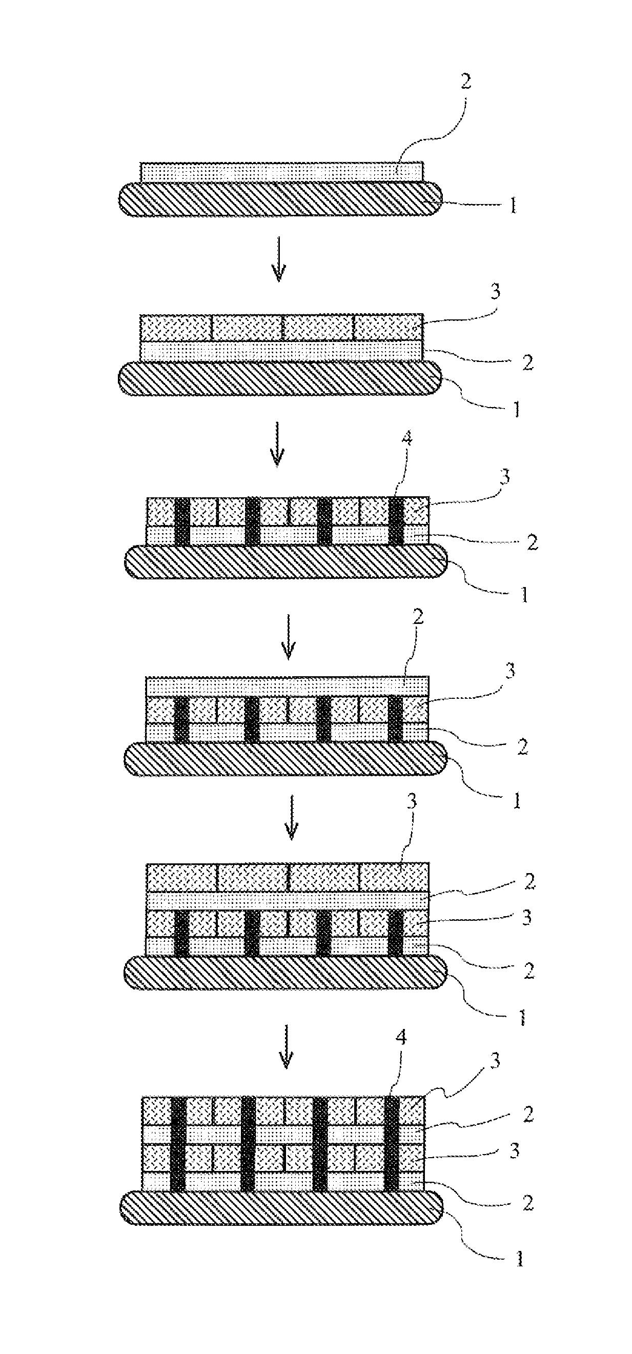
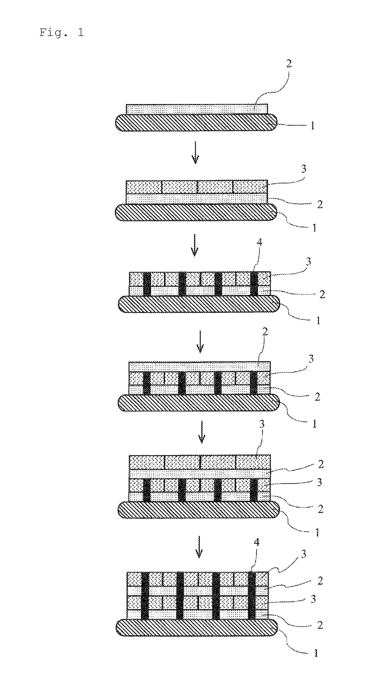
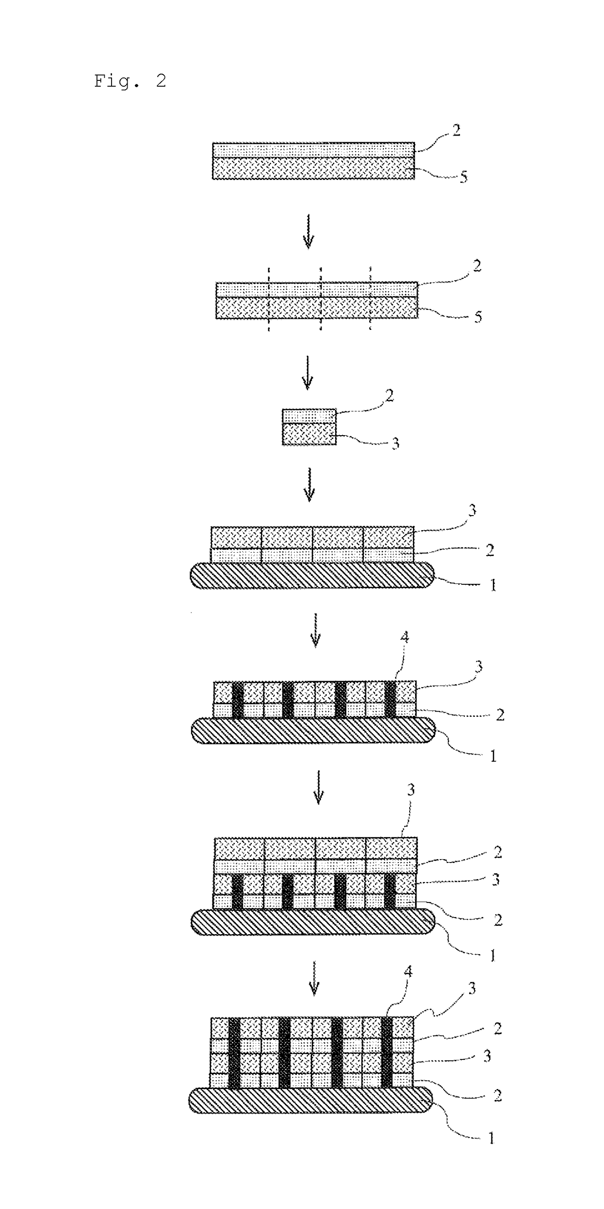
Image

Examples
example 1
[0201]There were used 450 g of 1,2-epoxy-4-(2-oxiranyl)cyclohexane adduct of 2,2-bis(hydroxymethyl)-1-butanol (softening point: 70° C. to 90° C., trade name EHPE3150, supplied by Daicel Corporation) and 50 g of (3,4,3′,4′-diepoxy)bicyclohexyl (melting point: 0° C. or lower), both as polymerizable compounds; 10 g of a PF6− sulfonium salt (trade name SI-150L, having a thermal curing time of 5.4 minutes at 130° C., supplied by SANSHIN CHEMICAL INDUSTRY CO., LTD.) as a cationic-polymerization initiator; 0.1 g of (4-hydroxyphenyl)dimethylsulfonium methylsulfate (Auxiliary for San-Aid SI Series, supplied by SANSHIN CHEMICAL INDUSTRY CO., LTD.) as a cationic-polymerization stabilizer; and 0.1 g of 3-glycidoxypropyltriethoxysilane (trade name KBE-403, supplied by Shin-Etsu Chemical Co., Ltd.) as a silane coupling agent. These were dissolved in 500 g of propylene glycol monomethyl ether acetate solvent and yielded an adhesive composition (1).
[0202]A silicon plate having a size of 2 cm by 5 c...
example 2
[0207]An adhesive composition (2) was prepared by a procedure similar to Example 1, except for using, as polymerizable compounds, 450 g of EHPE3150, 25 g of (3,4,3′,4′-diepoxy)bicyclohexyl, and 25 g of 1,4-bis[(3-ethyl-3-oxetanylmethoxy)methyl]benzene (melting point: 41° C., trade name OXT121, supplied by Toagosei Co., Ltd.).
[0208]Except for using the prepared adhesive composition (2), a silicon plate with adhesive layer (2) was prepared by a procedure similar to Example 1.
[0209]At a temperature of 30° C. or lower, the adhesive layer (2) had approximately no adhesiveness to another silicon plate and to a glass plate and could be cut without adhesive deposition on a box cutter blade. The adhesive layer (2) was found to have a complex viscosity of 0.21 Pa·s at 80° C.
[0210]Immediately after the formation of the adhesive layer (2), a glass plate was placed on the silicon plate with the adhesive layer (2) and was compressed at 600 Kgf / m2 at 80° C. in a reduced-pressure atmosphere for 5 m...
example 3
[0214]An adhesive composition (3) was prepared by a procedure similar to Example 1, except for not using the Auxiliary for San-Aid SI Series as the cationic-polymerization stabilizer.
[0215]Except for using the prepared adhesive composition (3), a silicon plate with adhesive layer (3) was prepared by a procedure similar to Example 1.
[0216]At a temperature of 30° C. or lower, the adhesive layer (3) had approximately no adhesiveness to another silicon plate and to a glass plate and could be cut without adhesive deposition on a box cutter blade. The adhesive layer (3) was found to have a complex viscosity of 0.25 Pa·s at 80° C.
[0217]Immediately after the formation of the adhesive layer (3), a glass plate was placed on the silicon plate with adhesive layer (3) and compressed at 600 Kgf / m2 at 80° C. in a reduced-pressure atmosphere for 5 minutes, by a procedure similar to Example 1. This allowed the adhesive layer (3) to soften and to adhere to the adherend. The resulting article was heat...
PUM
| Property | Measurement | Unit |
|---|---|---|
| melting point | aaaaa | aaaaa |
| temperature | aaaaa | aaaaa |
| temperature | aaaaa | aaaaa |
Abstract
Description
Claims
Application Information