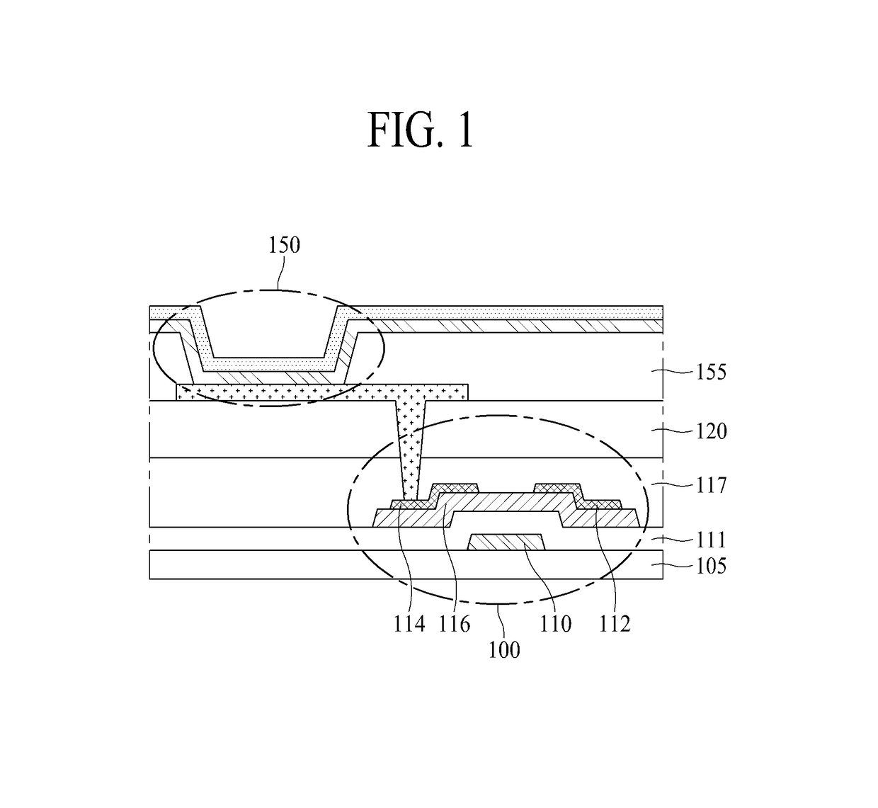
Organic light emitting device
a light-emitting device and organic technology, applied in the direction of semiconductor devices, basic electric elements, electrical appliances, etc., can solve the problems of shortened lifespan of organic light-emitting devices, lowering emission efficiency, and limiting so as to improve emission efficiency and lifespan, reduce the effect of high driving voltag
- Summary
- Abstract
- Description
- Claims
- Application Information
AI Technical Summary
Benefits of technology
Problems solved by technology
Method used
Image

Examples
first embodiment
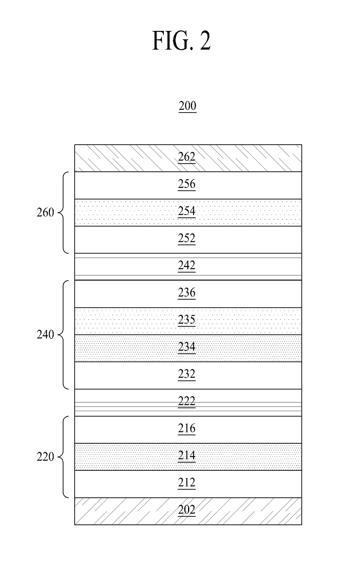
[0061]FIG. 2 is a cross sectional view illustrating an organic light emitting device 200 according to the present invention.
[0062]Referring to FIG. 2, the organic light emitting device 200 may include an anode 202, a first emitting part 220, a second emitting part 240, a third emitting part 260, and a cathode 262.
[0063]The anode 202 is electrically connected with the thin film transistor described with reference to FIG. 1 via a contact hole. The anode 202 is an electrode for injecting a hole with a positive charge to an emission layer. For an easy injection of the hole with the positive charge, the anode 202 may be formed of a transparent material such as ITO (Indium Tin Oxide) or IZO (Indium Zinc Oxide).
[0064]The anode 202 serves as a transparent layer in a bottom emission type, and also serves as a reflection layer in a top emission type.
[0065]The cathode 262 is provided at the opposite side of the anode 202 in the organic light emitting device 200. The cathode 262 is an electrode...
second embodiment
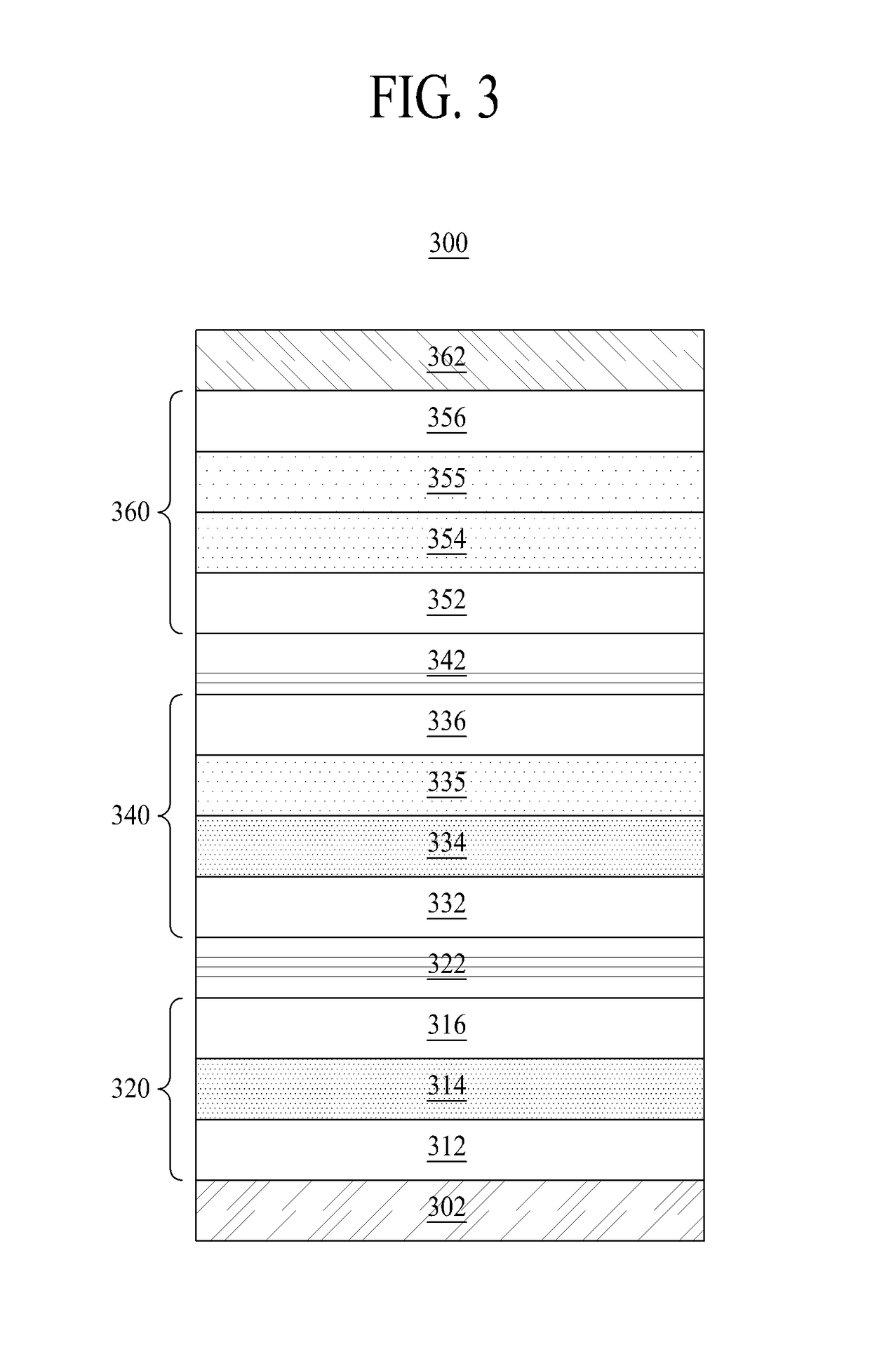
[0088]FIG. 3 is a cross sectional view illustrating an organic light emitting device 300 according to the present invention.
[0089]Referring to FIG. 3, the organic light emitting device 300 according to the second embodiment of the present invention may include an anode 302, a first emitting part 320, a second emitting part 340, a third emitting part 360, and a cathode 362. In addition, the organic light emitting device 300 according to the second embodiment of the present invention may further include an electron injection layer for a smooth injection of electron from the cathode 362, and a hole injection layer for a smooth injection of hole from the anode 302.
[0090]Also, a first charge generation layer 322 is additionally provided between the first emitting part 320 and the second emitting part 340, and a second charge generation layer 342 is additionally provided between the second emitting part 340 and the third emitting part 360.
[0091]The anode 302, the first emitting part 320, ...
third embodiment
[0098]FIG. 4 is a cross sectional view illustrating an organic light emitting device 400 according to the present invention.
[0099]Referring to FIG. 4, the organic light emitting device 400 according to the third embodiment of the present invention may include an anode 402, a first emitting part 420, a second emitting part 440, a third emitting part 460, and a cathode 462. The organic light emitting device 400 according to the third embodiment of the present invention may further include an electron injection layer for a smooth injection of electron from the cathode 462, and a hole injection layer for a smooth injection of hole from the anode 402. Also, a first charge generation layer 422 may be additionally provided between the first emitting part 420 and the second emitting part 440, and a second charge generation layer 442 may be additionally provided between the second emitting part 440 and the third emitting part 460.
[0100]A function and structure of the anode 402, the first emi...
PUM
 Abstract
Description
Claims
Application Information
 - R&D
- Intellectual Property
- Life Sciences
- Materials
- Tech Scout
- Unparalleled Data Quality
- Higher Quality Content
- 60% Fewer Hallucinations
Browse by: Latest US Patents, China's latest patents, Technical Efficacy Thesaurus, Application Domain, Technology Topic, Popular Technical Reports.
© 2025 PatSnap. All rights reserved.Legal|Privacy policy|Modern Slavery Act Transparency Statement|Sitemap|About US| Contact US: help@patsnap.com