Perovskite nanocrystalline particles and optoelectronic device using same

a technology of perovskite and nanocrystal particles, which is applied in the field of perovskite materials, can solve the problems of difficult uniform control of the intrinsic limitations of existing organic light-emitters, and the inability to uniformly control the size of the quantum dots, so as to improve the luminescence efficiency at room temperature, reduce the length of exciton diffusion, and high color purity

Active Publication Date: 2019-01-29
SN DISPLAY CO LTD
View PDF10 Cites 6 Cited by
  • Summary
  • Abstract
  • Description
  • Claims
  • Application Information

AI Technical Summary

Benefits of technology

[0043]The perovskite nanocrystal structure having the crystal structure, in which the FCC and the BCC are combined with each other, may be formed in the organic-inorganic-hybrid perovskite or inorganic metal halide perovskite nanocrystal particles, and the organic (or A site) plane and the inorganic plane may be alternately stacked to form the lamellar structure. Particularly, since the organic ammonium without having the conjugated structure is used as the organic material, the excitons may be confined to the inorganic plane to implement the high color purity.
[0044]According to the present invention, the bandgap energy of the organic-inorganic-hybrid perovskite nanocrystal particles or the inorganic metal halide perovskite nanocrystal particles may be determined by the perovskite crystal structure, unlike that the bandgap energy of inorganic quantum dot light-emitter depends on the particle size. Thus, since the particle size is greater than the range of the quantum confinement effect, the emission color may not be changed or slightly changed according to the particle size.
[0045]Also, the exciton diffusion length may be reduced, and the exciton binding energy may increase in the nanocrystal particle having a size of 10 nm to 30 nm to prevent the excitons from being annihilated by thermal ionization and the delocalization of the charge carriers, thereby luminescence efficiency at room temperature is improved.
[0046]Also, the organic-inorganic-hybrid perovskite nanocrystal particles or the inorganic metal halide perovskite nanocrystal particles may be nanoparticles that are dispersible in the organic solvent and thus applied to the various optoelectronic devices.
[0047]Also, the organic-inorganic-hybrid perovskite nanocrystal particles or the inorganic metal halide perovskite nanocrystal particles may be doped to increase the luminescence efficiency and the durability (or stability) as well as convert the semiconductor type into the n-type or the p-type, and thereby to adjust the opto-electrical properties.

Problems solved by technology

However, in terms of materials, both the organic light-emitters and the inorganic quantum dot light-emitters have intrinsic limitations.
The existing organic light-emitters have an advantage of high efficiency, but the existing organic light-emitters have a wide spectrum and poor color purity.
There is a problem that it is difficult to uniformly control the sizes of the quantum dots as the color approaches the blue color, and thereby the size distribution deteriorates the color purity because of size distribution.
Furthermore, because the inorganic quantum dots have a very deep valence band, there is a problem that it is difficult to inject holes because a hole injection barrier from an organic hole injection layer or an anode is too large.
Also, both the light-emitters (organic emitters and inorganic quantum dot emitters) are disadvantageously expensive.
Therefore, the organic-inorganic-hybrid perovskite are unsuitable for a light emitting layer.
Thus, in this case, it is not very suitable for the light-emitter having the high color purity, which is highlighted in this patent.
However, since the organic-inorganic-hybrid perovskite or the inorganic metal halide perovskite has small exciton binding energy, there is a fundamental problem that the luminescence occurs at a low temperature, but the excitons do not efficiently emit light at room temperature due to thermal ionization and delocalization of a charge carrier and thus they are easily separated as free charge carriers and then annihilated.
Also, there is a problem in that the excitons are annihilated by the layer having high conductivity in the vicinity of the excitons when the free charge carriers are recombined again to form excitons.

Method used


Image

  • Perovskite nanocrystalline particles and optoelectronic device using same
  • Perovskite nanocrystalline particles and optoelectronic device using same
  • Perovskite nanocrystalline particles and optoelectronic device using same

Examples


manufacturing example 1

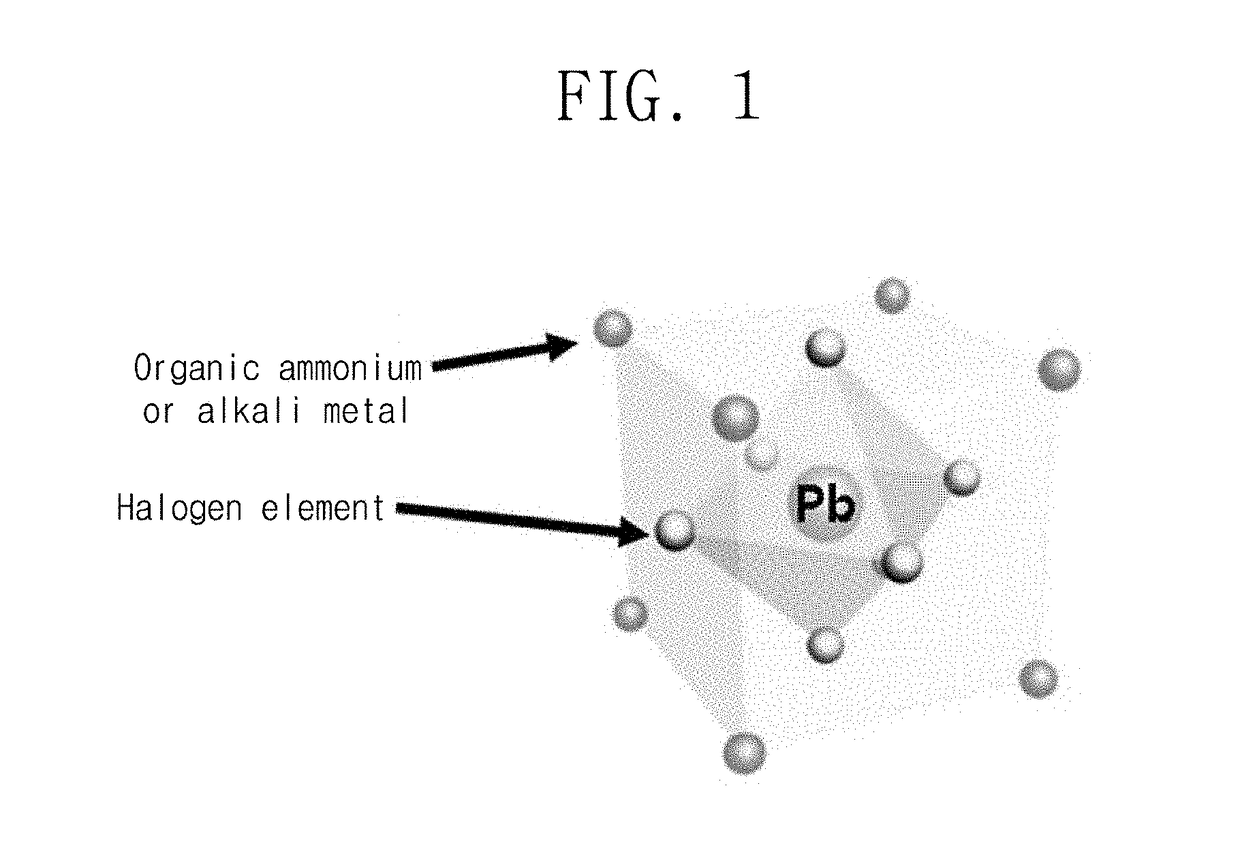
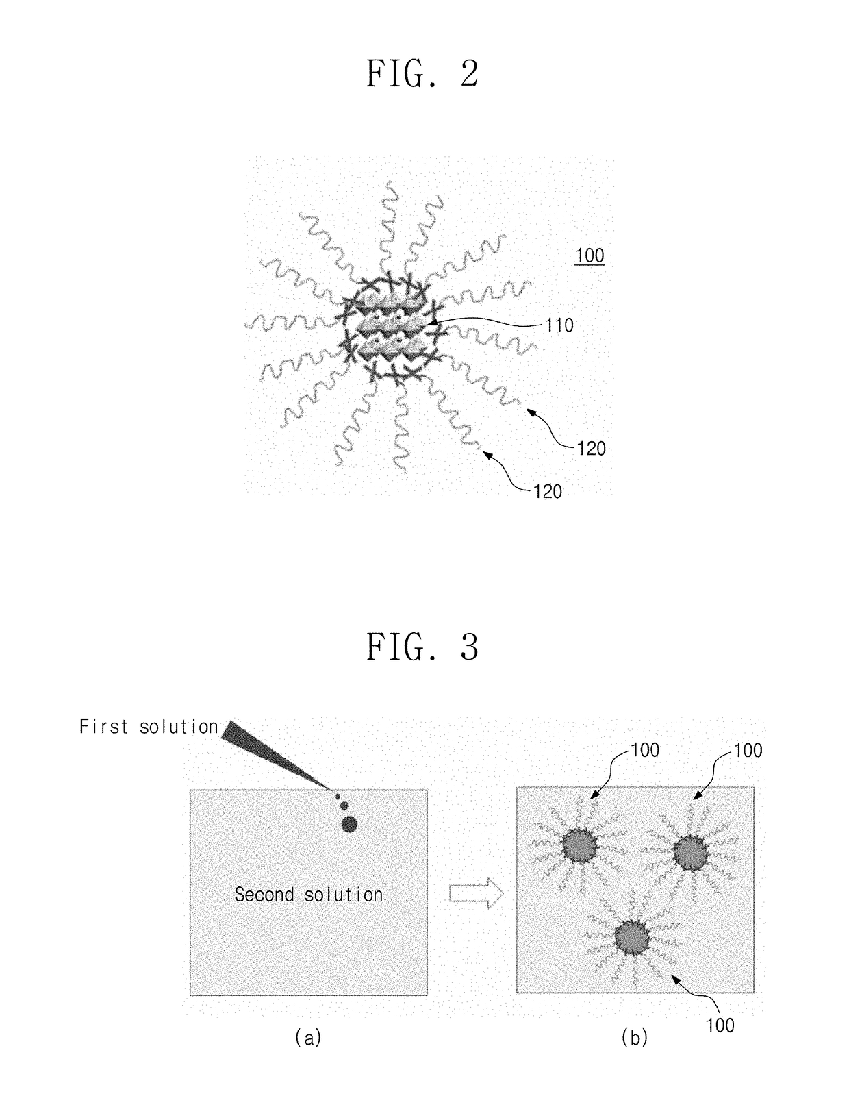
[0209]An organic-inorganic-hybrid perovskite nanocrystal particle having a 3D structure according to an embodiment of the present invention was formed. The organic-inorganic-hybrid perovskite nanocrystal particle was formed through an inverse nano-emulsion method, reprecipitation method or hot-injection method.

[0210]Particularly, organic-inorganic-hybrid perovskite was dissolved in a polar solvent to prepare a first solution. Here, dimethylformamide was used as the polar solvent, and CH3NH3PbBr3 was used as the organic-inorganic-hybrid perovskite. Here, the used CH3NH3PbBr3 was prepared by mixing CH3NH3Br with PbBr2 at a ratio of 1:1.

[0211]Also, a second solution in which an alkyl halide surfactant is dissolved in a non-polar solvent was prepared. Here, toluene was used as the non-polar solvent, and octadecylammonium bromide (CH3(CH2)17NH3Br) was used as the alkyl halide surfactant.

[0212]Then, the first solution slowly dropped drop-wisely into the second solution that is being stron...

manufacturing example 2

[0215]The same process as that according to Manufacturing Example 1 was performed, and CH3(CH2)13NH3Br was used as an alkyl halide surfactant to form an organic-inorganic-hybrid perovskite nanocrystal particle having a 3D structure according to an embodiment of the present invention.

[0216]Here, the formed organic-inorganic-hybrid perovskite nanocrystal particle has a size of about 30 nm on average.

manufacturing example 3

[0217]The same process as that according to Manufacturing Example 1 was performed, and CH3(CH2)10NH3Br was used as an alkyl halide surfactant to form an organic-inorganic-hybrid perovskite nanocrystal particle having a 3D structure according to an embodiment of the present invention.

[0218]Here, the formed organic-inorganic-hybrid perovskite nanocrystal particle has a size of about 40 nm on average.


PUM

PropertyMeasurementUnit
diameteraaaaaaaaaa
emission wavelengthaaaaaaaaaa
bandgap energyaaaaaaaaaa

Abstract

Provided are perovskite nanocrystalline particle and an optoelectronic device using the same. The perovskite nanocrystalline particle may include a perovskite nanocrystalline structure while being dispersible in an organic solvent. Accordingly, the perovskite nanocrystalline particle in accordance with the present invention has therein a perovskite nanocrystal having a crystalline structure in which FCC and BCC are combined; can form a lamellar structure in which an organic (or A site) plane and an inorganic plane are alternately stacked; and can show high color purity since excitons are confined to the inorganic plane.

Description

TECHNICAL FIELD[0001]The present invention relates to a perovskite material, and more particularly, to an organic-inorganic-hybrid perovskite or inorganic metal halide perovskite nanocrystal particles and an optoelectronic device using the same.BACKGROUND ART[0002]The major trend of the display market is shifting from the existing high-efficiency and high-resolution-oriented display to the emotional image-quality display aiming at realizing a high color purity for demonstration of natural colors. From this viewpoint, while organic light emitting diode (OLED) devices using organic light-emitters have remarkably developed, inorganic quantum dot LEDs with the improved color purity have been actively researched and developed as alternatives. However, in terms of materials, both the organic light-emitters and the inorganic quantum dot light-emitters have intrinsic limitations.[0003]The existing organic light-emitters have an advantage of high efficiency, but the existing organic light-em...

Claims


Application Information

Patent Timeline
Patent Type & Authority Patents(United States)
IPC IPC(8): H01L51/00C09K11/02C01G21/16C09K11/66C07F7/24C09K11/06H01L51/56H01L51/50B82Y30/00H01L51/44B82Y40/00H01L51/52H01L51/42B82Y20/00
CPCH01L51/0077C07F7/24C09K11/02C09K11/025C09K11/06C09K11/665H01L51/004H01L51/0037H01L51/0072C01G21/16Y10S977/95B82Y20/00B82Y30/00B82Y40/00C01P2002/34C01P2002/60C01P2004/64C01P2004/80C01P2006/40C09K2211/188H01L51/424H01L51/442H01L51/5012H01L51/5206H01L51/5221H01L51/56H01L2251/301H01L2251/308H01L2251/558Y10S977/774Y10S977/788Y10S977/814Y10S977/892Y10S977/896Y10S977/948C07C211/03C07C211/04C09K11/664C09K2211/10H10K85/60H10K50/115C01G21/006C01P2004/84Y02E10/549H10K85/30H10K50/11H10K85/50H10K85/141H10K85/1135H10K85/6572H10K30/20H10K30/82H10K50/81H10K50/82H10K71/00H10K2102/00H10K2102/103H10K2102/351
Inventor LEE, TAE-WOOIM, SANGHYUKKIM, YOUNG-HOONCHO, HIMCHAN
Owner SN DISPLAY CO LTD
Why Eureka
Try Eureka