Systems and methods for metrology beam stabilization

a technology of metrology and beam stabilization, applied in the field of metrology systems and methods, can solve the problems of reducing the measurement range, reducing the measurement box size, and reducing the size of the measurement box

Active Publication Date: 2019-07-30
KLA CORP
View PDF69 Cites 6 Cited by
  • Summary
  • Abstract
  • Description
  • Claims
  • Application Information

AI Technical Summary

Benefits of technology

[0012]Methods and systems for measuring a specimen while actively stabilizing an optical measurement beam subject to changes in polarization by a rotating polarizer element are described herein. Movement of a focused measurement beam spot induced by a rotating polarizer element is compensated by actively controlling the position of an optical element in the beam path based on measurements of the focused measurement beam spot. By reducing the movement of the measurement beam spot, optical measurements of a semiconductor structure are achieved with a reduced measurement box size.
[0013]By actively controlling measurement beam movement induced by a rotating polarizer element, wedge error tolerances on polarizer elements may be increased along with rotary bearing tolerances. This increases design flexibility and reduces cost. In addition, active control of measurement beam movement compensates for effects such as temperature shift and bearing wear. In addition, optical system alignment may be checked while the measurement system is running by monitoring measurement beam location and movement.
[0014]In one aspect, a measurement system includes a rotating optical polarizer, a beam position sensor, and an active beam compensating element in the illumination beam path, the collection beam path, or both. Beam position errors induced by the rotary motion of the rotating optical polarizer are detected by the beam position sensor. A computing system communicates control commands to the active beam compensating element, and, in response, the active beam compensating element adjusts a location of the measurement beam to reduce the beam position errors as detected by the beam position sensor.
[0017]In general, both feedback and feedforward control schemes as described herein may be employed simultaneously to reduce beam position error.

Problems solved by technology

However, it remains a challenge to preserve a small measurement box size.
In the semiconductor industry, where wafer space allocated to metrology targets is limited (often, within the scribe line or even within die), the desired box size specification can be often very challenging, such as 30 μm×30 μm, 10 μm×10 μm, or even smaller.
Despite existing approaches designed to control measurement box size, achieving a small measurement box size specification over the full measurement range is very challenging.
In addition, the mechanical bearings employed to constrain the rotational motion of the polarization optics have finite concentricity and runout errors.
This causes the polarization optics to wobble about the optical axis of a beam passing through the polarization optics.
Wedge errors and rotary bearing errors change the optical path of the beam relative to other optical elements in the system.
This manifests itself as beam positioning errors at various critical locations in the optical path.
For example, for a spectroscopic ellipsometer system, wedge errors and rotary bearing errors cause misalignment of the optical beam with a polarizer slit, the specimen under measurement, and a spectrometer slit as polarizing elements are rotated.
As the measurement spot moves during rotation of polarizing elements, measurement precision, accuracy, and matching among multiple tools suffers.
However, there are practical, manufacturing limits on achievable wedge error tolerance, particularly within reasonable cost.
In addition, even if it were possible to manufacture a polarizer element with zero wedge error, changes in environmental conditions (e.g., temperature) cause the wedge angle to change, resulting in movement of the measurement spot during rotation of the polarizer element.
Again, there are practical, manufacturing limits on achievable runout error tolerance, particularly within reasonable cost.
In addition, even if it were possible to manufacture bearings with perfect concentricity and zero runout, bearing wear causes increasing error over time, particularly over the lifetime of semiconductor metrology tool subject to near constant use.
This approach is not effective if the beam passing through the polarizer optic is collimated.
Also, this approach does not work as well if there are two rotating polarizer optics in the beam path.
In addition, this approach is not effective when bearings wear over time or wedge errors change with temperature.
As lithographic and metrology systems are pressed to higher resolutions, measurement box size becomes a limiting factor in maintaining device yield.

Method used


Image

  • Systems and methods for metrology beam stabilization
  • Systems and methods for metrology beam stabilization
  • Systems and methods for metrology beam stabilization

Examples


Embodiment Construction

[0036]Reference will now be made in detail to background examples and some embodiments of the invention, examples of which are illustrated in the accompanying drawings.

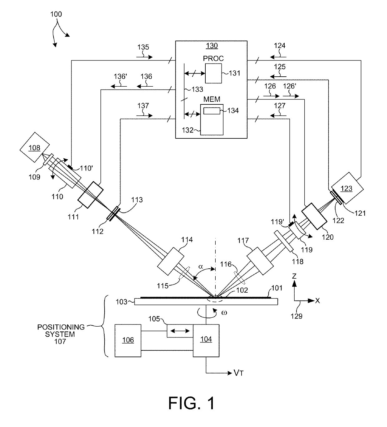
[0037]Methods and systems for measuring a specimen while actively stabilizing an optical measurement beam subject to changes in polarization by a rotating polarizer element are described herein. Movement of a focused measurement beam spot induced by a rotating polarizer element is compensated by actively controlling the position of an optical element in the beam path based on measurements of the focused measurement beam spot. By reducing the movement of the measurement beam spot, optical measurements of a semiconductor structure are achieved with a reduced measurement box size.

[0038]By actively controlling measurement beam movement induced by a rotating polarizer element wedge error tolerances on polarizer elements may be increased along with rotary bearing tolerances. This increases design flexibility and reduces cos...


PUM

PropertyMeasurementUnit
sizeaaaaaaaaaa
sizeaaaaaaaaaa
wavelengthaaaaaaaaaa

Abstract

Methods and systems for measuring a specimen while actively stabilizing an optical measurement beam subject to changes in polarization by a rotating polarizer element are described herein. Movement of a focused measurement beam spot induced by a rotating polarizer element is compensated by actively controlling the position of an optical element in the beam path based on measurements of the focused measurement beam spot. Both feedback and feedforward control schemes may be employed to reduce beam position error. In one aspect, a measurement system includes a rotating optical polarizer, a beam position sensor, and an active beam compensating element in the illumination beam path, the collection beam path, or both. Beam position errors are detected by the beam position sensor, and control commands are communicated to the active beam compensating element to reduce the measured beam position errors.

Description

TECHNICAL FIELD[0001]The described embodiments relate to metrology systems and methods, and more particularly to methods and systems for improved measurement resolution with smaller measurement box sizes.BACKGROUND INFORMATION[0002]Semiconductor devices such as logic and memory devices are typically fabricated by a sequence of processing steps applied to a specimen. The various features and multiple structural levels of the semiconductor devices are formed by these processing steps. For example, lithography among others is one semiconductor fabrication process that involves generating a pattern on a semiconductor wafer. Additional examples of semiconductor fabrication processes include, but are not limited to, chemical-mechanical polishing, etch, deposition, and ion implantation. Multiple semiconductor devices may be fabricated on a single semiconductor wafer and then separated into individual semiconductor devices.[0003]A lithographic process, as described above, is performed to se...

Claims


Application Information

Patent Timeline
Patent Type & Authority Patents(United States)
IPC IPC(8): G03F7/20G02B27/00G02B26/08G01N21/21G01B11/02
CPCG01N21/211G01B11/02G02B26/08G02B26/0816G02B27/0025G02B27/0075G03F7/70625G03F7/70633G02B26/0875G01N2021/213G01B2210/56G02B26/0883G01N21/8806G01B11/272G01N21/21G01N2021/8848G01N2201/0683
Inventor BLASENHEIM, BARRYSAPIENS, NOAMFRIEDMANN, MICHAEL
Owner KLA CORP
Why Eureka
Try Eureka