Microwave or millimeter wave RF part realized by die-forming

a technology of die-forming and microwaves, applied in the direction of waveguides, antennas, domestic articles, etc., can solve the problems of large losses in both dielectric and conductive parts of microstrip networks, high conductive losses due to miniaturization, and the inability to make microstrip lines only wider, etc., to achieve cost-effective production and good performan

Active Publication Date: 2019-12-03
GAPWAVES
View PDF16 Cites 5 Cited by
  • Summary
  • Abstract
  • Description
  • Claims
  • Application Information

AI Technical Summary

Benefits of technology

[0015]It is therefore an object of the present invention to alleviate the above-discussed problems, and specifically to provide a new waveguide and RF packaging technology, which has good performance and which is cost-efficient to produce, in particular for use above 30 GHz, and e.g. for use in an antenna system for use in communication, radar or sensor applications.

Problems solved by technology

The consumer market prefers flat antennas, and these can only be realized as flat planar arrays, and the wide bandwidth of these systems require corporate distribution network.
However, such microstrip networks suffer from large losses in both dielectric and conductive parts.
The dielectric losses do not depend on the miniaturization, but the conductive losses are very high due to the miniaturization.
Unfortunately, the microstrip lines can only be made wider by increasing substrate thickness, and then the microstrip network starts to radiate, and surface waves starts to propagate, both destroying performance severely.
However, the SIW technology still has significant dielectric losses, and low loss dielectric materials are very expensive and soft, and therefore not suitable for low-cost mass production.
This waveguide can have low dielectric and conductive losses, but it is not compatible with PCB technology.
The textured pin surface could be realized by mushrooms on a PCB, but this then becomes one of two PCB layers to realize the microstrip network, whereby it would be much more costly to produce than gap waveguides realized only using one PCB layer.
Also, there are many problems with this technology: It is difficult to find a good wideband way of connecting transmission lines to it from underneath.
It is expensive both to manufacture the periodic pin array under the microstrip feed network on the substrate located directly upon the pin surface, and the radiating elements which in this case were compact horn antennas.
It was very expensive to realize the PCBs with sufficient tolerances, and in particular to keep the air gap with constant height.
The microstrip-ridge gap waveguide also requires an enormous amount of thin metallized via holes that are very expensive to manufacture.
In particular, the drilling is expensive.

Method used


Image

  • Microwave or millimeter wave RF part realized by die-forming
  • Microwave or millimeter wave RF part realized by die-forming
  • Microwave or millimeter wave RF part realized by die-forming

Examples


Embodiment Construction

[0096]In the following detailed description, preferred embodiments of the present invention will be described. However, it is to be understood that features of the different embodiments are exchangeable between the embodiments and may be combined in different ways, unless anything else is specifically indicated. Even though in the following description, numerous specific details are set forth to provide a more thorough understanding of e present invention, it will be apparent to one skilled in the art that the present invention may be practiced without these specific details. In other instances, well-known constructions or functions are not described in detail, so as not to obscure the present invention.

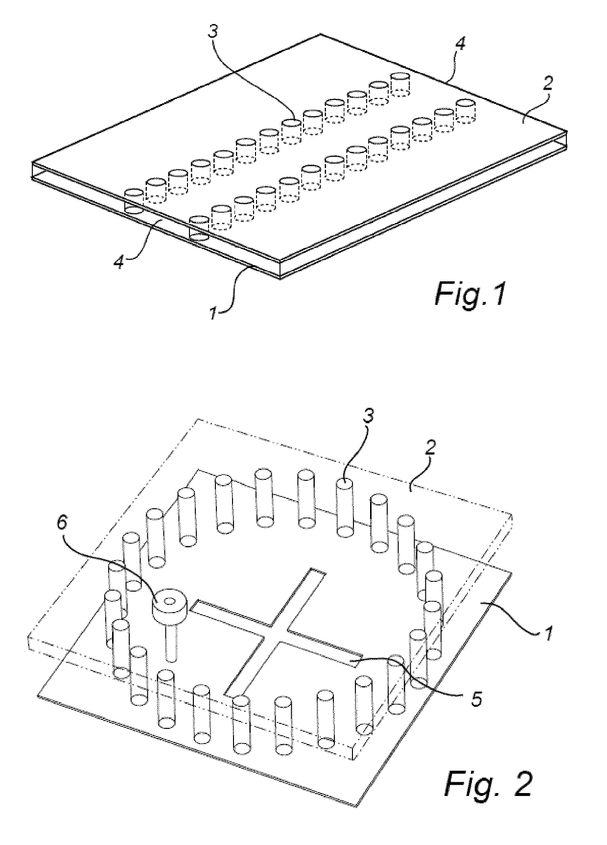
[0097]In a first embodiment, as illustrated in FIG. 1, an example of a rectangular waveguide is illustrated. The waveguide comprises a first conducting layer 1, and a second conducting layer 2 (here made semi-transparent, for increased visibility). The conducting layers are arranged ...


PUM


Abstract

A method and apparatus for producing an RF part of an antenna system is disclosed, as well as thereby producible RF parts. The RF part has at least one surface provided with a plurality of protruding elements. In particular, the RF part may be a gap waveguide. The protruding elements are monolithically formed and fixed on a conducting layer, and all protruding elements are connected electrically to each other at their bases via the conductive layer. The RF part is produced by providing a die having a plurality of recessions forming the negative of the protruding elements of the RF part. The die may be a multilayer die, having several layers, at least some having through-holes to form the recessions. A formable piece of material is arranged on the die, and pressure is applied, thereby compressing the formable piece of material to conform with the recessions of the die.

Description

TECHNICAL FIELD OF THE INVENTION[0001]The present invention relates to the technology used to design, integrate and package the radio frequency (RF) part of an antenna system, for use in communication, radar or sensor applications, and e.g. components such as waveguide couplers, diplexers, filters, antennas, integrated circuit packages and the like.BACKGROUND[0002]There is a need for technologies for fast wireless communication in particular at 60 GHz and above, involving high gain antennas, intended for consumer market, so low-cost manufacturability is a must. The consumer market prefers flat antennas, and these can only be realized as flat planar arrays, and the wide bandwidth of these systems require corporate distribution network. This is a completely branched network of lines and power dividers that feed each element of the array with the same phase and amplitude to achieve maximum gain.[0003]A common type of flat antennas is based on a microstrip antenna technology realized on...

Claims


Application Information

Patent Timeline
Patent Type & Authority Patents(United States)
IPC IPC(8): H01P3/123B21K23/00H01Q21/00H01P1/211H01Q21/06H01Q1/38H01P1/20H01Q13/10H01Q13/02H01Q21/20
CPCH01Q1/38H01Q21/0087H01Q21/005B21K23/00H01Q21/064H01P3/123H01P1/211H01Q13/106H01Q13/0283H01Q21/0037H01P1/2005H01Q13/10H01Q21/20
Inventor HADAVY, FARIDKILDAL, PER-SIMON
Owner GAPWAVES
Why Eureka
Try Eureka