

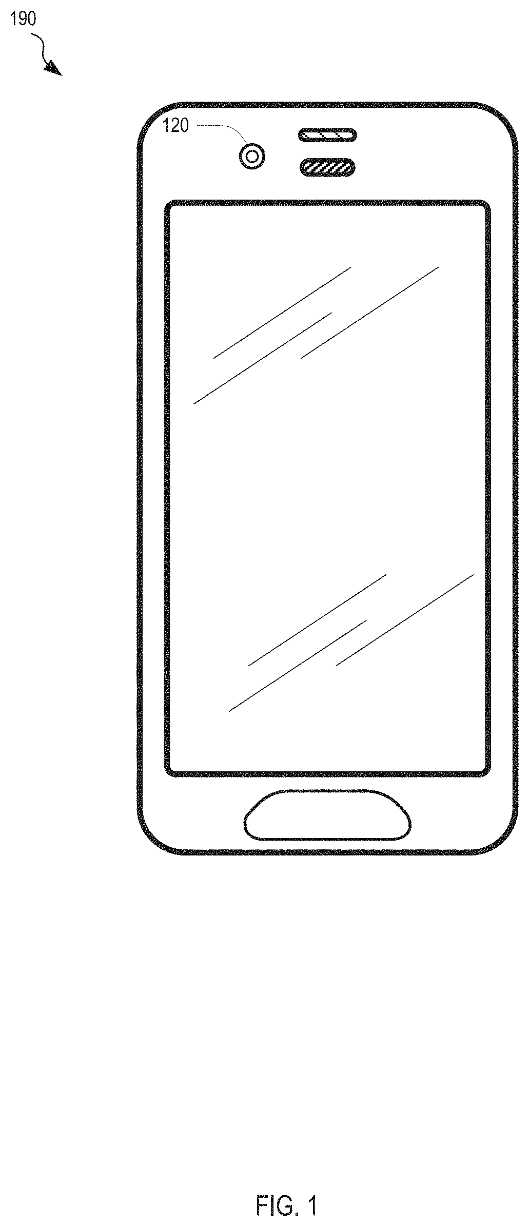
Plasmonic-nanostructure sensor pixel
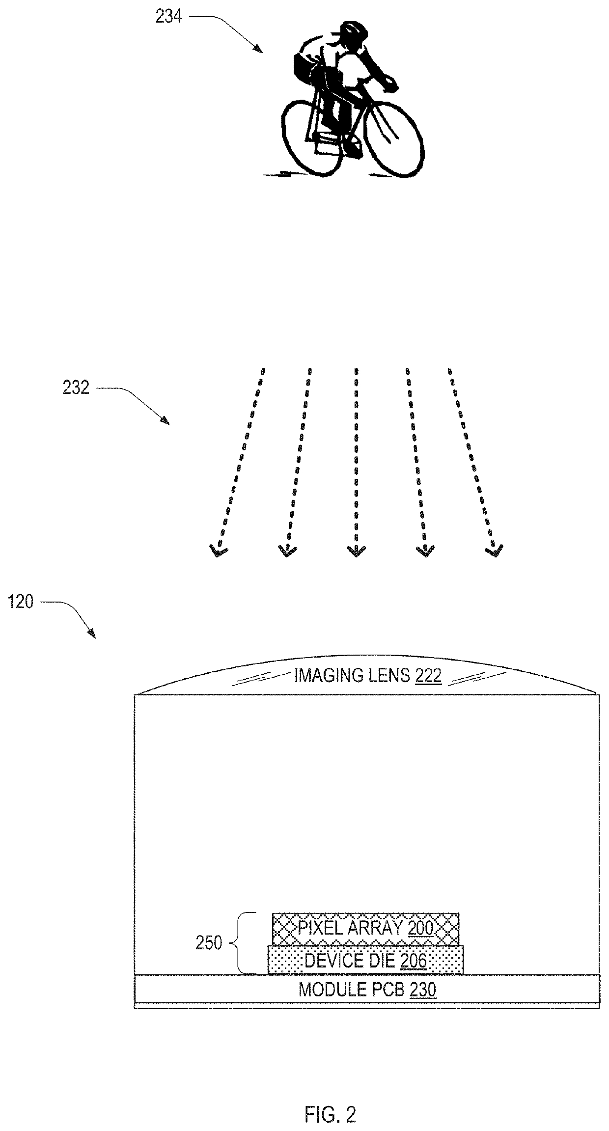
a sensor and nanostructure technology, applied in the field of low-cost complementary metaloxide semiconductor (cmos) image sensors, can solve the problem that the silicon substrate 320/b> absorbs infrared light much less efficiently than the visible ligh
- Summary
- Abstract
- Description
- Claims
- Application Information
AI Technical Summary
Benefits of technology
Problems solved by technology
Method used
Image

Examples
Embodiment Construction
[0019]FIGS. 4A and 4B are cross-sectional views of a plasmonic-nanostructure sensor pixel 400. Plasmonic-nanostructure sensor pixel 400 is compatible for use in pixel array 200. The cross-sectional view of FIG. 4A is in the x-z plane of a coordinate system 498. The cross-sectional view of FIG. 4B is along cross-section B-B′ of FIG. 4A and in the x-y plane of a coordinate system 498. Plasmonic-nano structure sensor pixel 400 includes a plurality of metal pillars 430 in a substrate 420 arranged in an array 439.
[0020]Substrate 420 is formed of a semiconductor such as silicon, and may include layers and regions of different materials without departing from the scope hereof. Metal pillars 430 may be formed of a noble metal such as aluminum, gold, silver, platinum, and copper, or an alloy thereof. Substrate 420 has a top surface 421, which may be planar as illustrated in FIG. 4A, or non-planar.
[0021]Plasmonic-nanostructure sensor pixel 400 may also include at least one of an insulating la...
PUM
| Property | Measurement | Unit |
|---|---|---|
| width | aaaaa | aaaaa |
| width | aaaaa | aaaaa |
| distance | aaaaa | aaaaa |
Abstract
Description
Claims
Application Information