Low voltage rail to rail high speed analog buffer and method thereof

a high-speed analog buffer and low-voltage rail technology, applied in push-pull amplifiers, single-ended push-pull amplifiers, phase splitters, etc., can solve the problems of increasing the current consumption of the (inverting) buffer driver, consuming current itself, and affecting the operation of the buffer, so as to reduce the minimum operating power supply and reduce the offset of the amplifier

Active Publication Date: 2020-01-14
FAR ALI TASDIGHI
View PDF88 Cites 21 Cited by
  • Summary
  • Abstract
  • Description
  • Claims
  • Application Information

AI Technical Summary

Benefits of technology

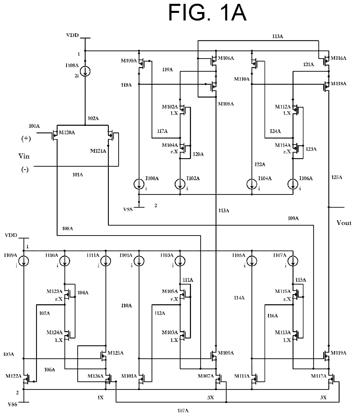
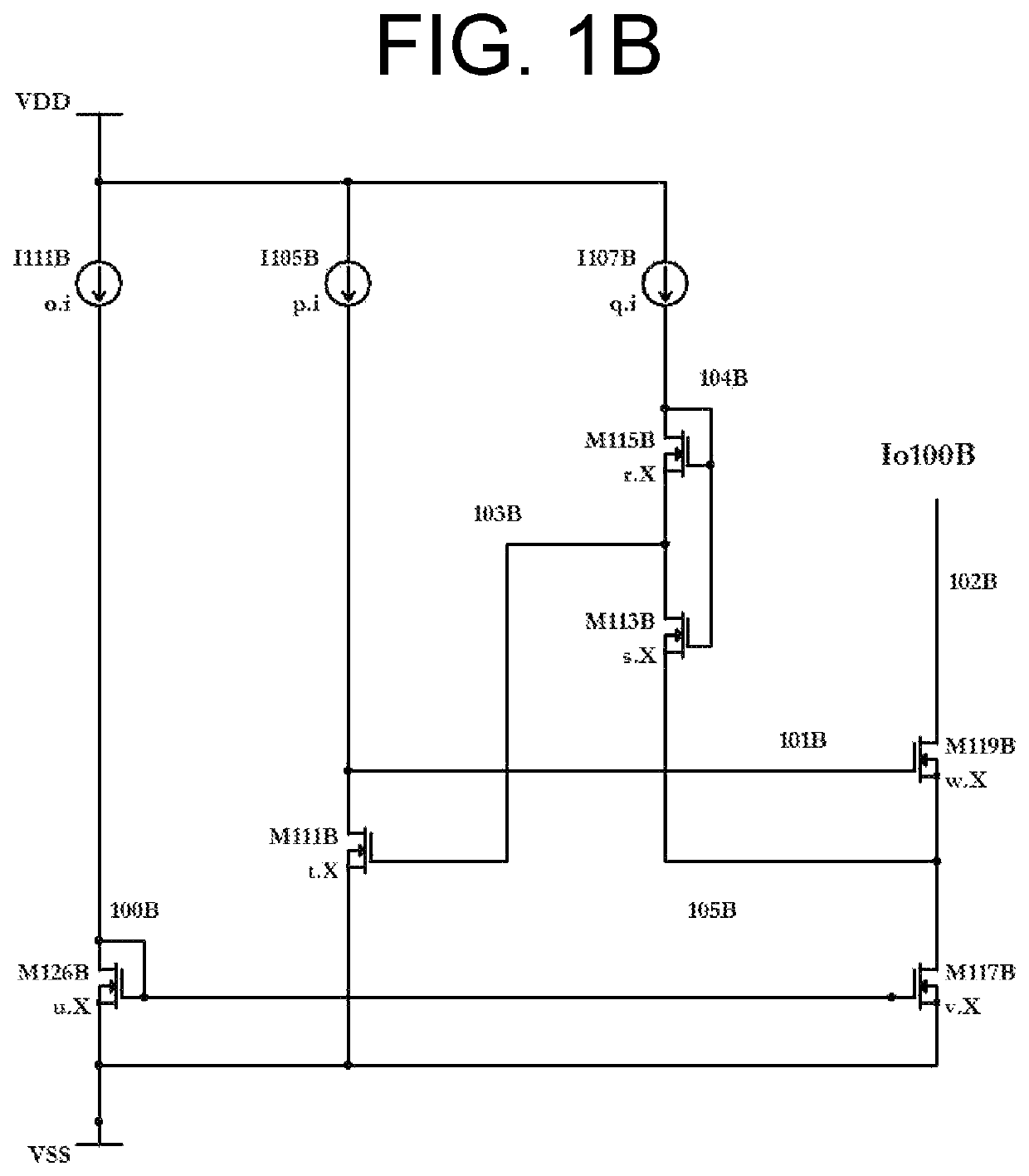
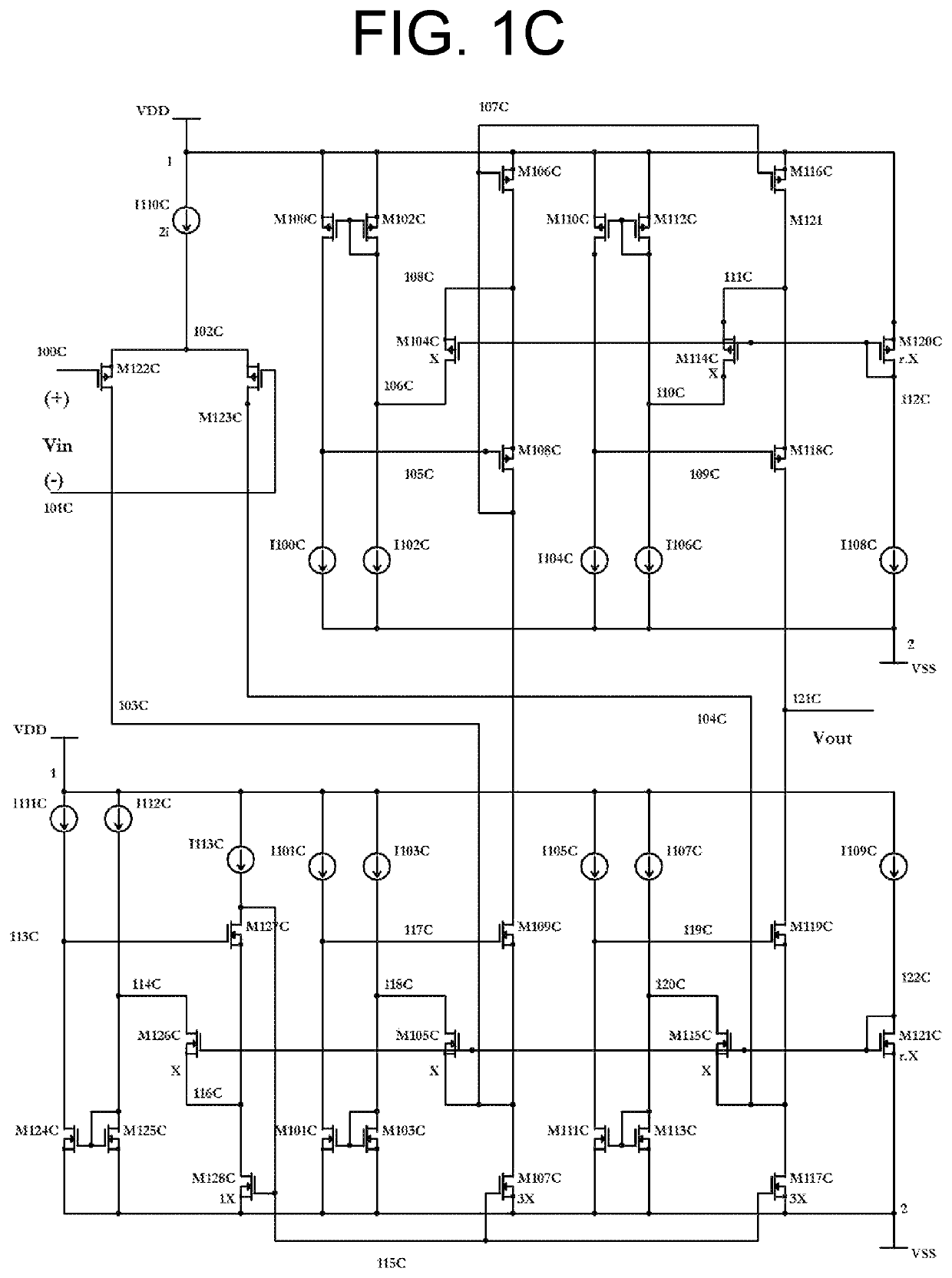
[0004]An aspect of the present disclosure is to make small and low cost current sources, current mirrors, amplifiers, buffers drivers, and buffer amplifiers that can operate with one or more of the following characteristics: (a) wide input-output voltage span, (b) low power supply voltage, (c) low power consumption, (d) low noise, (e) fast dynamic response, (f) symmetric design to minimize systematic errors, (g) use simple design that generally improves performance to specifications over operating and process variation, and / or (h) make the IC rugged for long term manufacturing using standard CMOS fabrication process that is inexpensive, and readily available at multiple fabrication factories, thus easing process node portability.

Problems solved by technology

Given that the sink-source currents of FET400B can vary significantly, depending on the external load, the scaled down but un-rectified mirroring of FET400B raw currents can also vary a lot, and increase the current consumption of a (inverting) buffer driver.
First, the function of ‘monitoring’, of sink-source currents, consume current itself.
Sink-source currents can be high and have unpredictable patterns.
Second, the buffer driver is fast since the CNICM couple with MCS coupled with ICMA are all in principal operating in current mode, which is inherently fast.
First, the function of ‘monitoring’, of sink-source currents, consumes current itself.
Sink-source currents can be high and have unpredictable patterns.
Second, the buffer driver is fast since the CNICM couple with LTA coupled with CMA are all in principal operate in current mode, which is inherently fast.
Second, it principally operates in current mode which makes it inherently fast.
Fourth, it can run at ultra low currents, which makes its power consumption ultra-low when combined with its ability to perform to specifications with low power supply voltage.
Moreover, the ICMA has a high output impedance that, when connected to an amplifier's gain stage, it neither substantially loads the amplifier's high impedance node nor does it dynamically slow the amplifier.

Method used


Image

  • Low voltage rail to rail high speed analog buffer and method thereof
  • Low voltage rail to rail high speed analog buffer and method thereof
  • Low voltage rail to rail high speed analog buffer and method thereof

Examples


first embodiment

Section (VII): Detailed Description of First Embodiment of an Amplifier of FIG. 2A Utilizing the First Floating Current Source (FCS200A)

[0129]FIG. 2A is a schematic circuit diagram of the embodiment illustrating an amplifier utilizing the first FCS (FCS200A) shown in BLOCK: FCS200A at the left bottom side of FIG. 2A. The embodiment discloses FCS200A, which emulates the benefits of a FCS in the amplifier current mirror network, enables the amplifier to operate at low VDD≤˜VGS+2VDS, improves matching of upper and lower currents independent of the common mode voltage swings.

[0130]The amplifier of FIG. 2A is a conventional folded cascode transconductance amplifier (FCTA) that utilizes FCS200A. As indicated in prior sections, broadly speaking, a FCTA is composed of a CSA that converts the input differential voltage to differential currents which are then fed onto a differential input and differential output CGA that is fast. In a FCTA, the differential current outputs of CGA are then ste...

second embodiment

Section (VIII): Detailed Description of Second Embodiment of an Amplifier of FIG. 2B Utilizing the Second Floating Current Source (FCS200B)

[0141]FIG. 2B is a schematic circuit diagram of the embodiment illustrating an amplifier utilizing the second FCS, which is depicted in BLOCK: FCS200B at the left bottom side of FIG. 2B. Similar to the first FCS discussed in the previous sections, the disclosed FCS200B, emulating the function of a floating current mirror in the amplifier's current mirror network, here that enables the amplifier to operate at low VDD≥˜VGS+2VDS, improves speed, and improve accuracy by making the current matching more independent of common mode voltage swings. Refer to the description provided regarding the FCTA of FIG. 2A in the previous section, which is similar to the amplifier herein FIG. 2B that utilizes FCS200B. The FCS200B illustrated in BLOCK: FCS200B (at the left bottom side of FIG. 2B) which also utilizes two cascode current sources, PMOSFETs (M200B and M2...

third embodiment

Section (IX): Detailed Description of Third Embodiment of an Amplifier of FIG. 2C Utilizing the Third Floating Current Source (FCS200C)

[0153]FIG. 2C is a schematic circuit diagram of the embodiment illustrating an amplifier utilizing the third FCS, which is depicted in BLOCK: FCS200C at the left bottom side of FIG. 2C. Similar to the FCSs discussed in previous sections, the disclosed FCS200B emulates the function of floating current source in the amplifier's current mirror network, here and enables the amplifier to operate at low VDD≥˜VGS+2VDS, and improve accuracy by making current matching more independent of common mode swings.

[0154]As just noted, from a high level functional perspective, the embodiment of FCS200C here is similar to that of FCS200A and FCS200C disclosed in the previous sections. The embodiment of the FCS200C is illustrated in BLOCK: FCS200B (at the left bottom side of FIG. 2C) which also utilizes two cascode current sources, PMOSFETs (M200C and M202C) and NMSOFET...


PUM


Abstract

Methods, circuits, and apparatuses that provide Buffer Amplifier, containing Amplifiers and Buffer Drivers, one or more of the following: ultra low power Buffer Amplifier, capable of having high gain, low noise, high speed, near rail-to-rail input-output voltage span, high sink-source current drive capability for an external load, and able to operate at low power supply voltages. Methods, circuits, and apparatuses that provide regulated cascode (RGC) current mirrors (CM) capable of operating at low power supply and having wide input-output voltage spans.

Description

CROSS-REFERENCE TO RELATED PATENT APPLICATIONS[0001]This application claims the priority benefit of U.S. patent application Ser. No. 15 / 451,334, filed Mar. 6, 2017 and entitled Ultra Low Power High-Performance Amplifier”; U.S. Provisional Patent Application Ser. No. 62 / 304,373, filed Mar. 7, 2016 and entitled “Class AB amplifier low power and fast”; U.S. Provisional Patent Application Ser. No. 62 / 320,512 filed Apr. 9, 2016 and entitled “Class AB amplifier high gain”; and U.S. Provisional Patent Application Ser. No. 62 / 415,496 filed Oct. 13, 2016 and entitled “Class AB Amplifier Low Noise”; Each of the above applications are herein specifically incorporated by reference in their entirety.FIELD OF DISCLOSURE[0002]This disclosure related to improvements in current mirrors, current sources, amplifiers, and output buffer drives for use in integrated circuits (ICs).BACKGROUND[0003]Operating ICs under ultra low currents and low power supplies, in complementary metal-oxide semiconductor (CM...

Claims


Application Information

Patent Timeline
Patent Type & Authority Patents(United States)
IPC IPC(8): H03F3/04H03F3/45H03F3/30H03F3/26H03F1/56H03F1/02
CPCH03F3/301H03F1/0244H03F3/45273H03F3/26H03F3/45192H03F1/56H03F3/45928H03F3/45475H03F2203/45426
Inventor FAR, ALI TASDIGHI
Owner FAR ALI TASDIGHI
Why Eureka
Try Eureka