
Organic light-emitting diode, organic light-emitting display including the same, and method of manufacturing the same

a technology of organic light-emitting diodes and light-emitting displays, which is applied in the direction of organic semiconductor devices, solid-state devices, semiconductor devices, etc., can solve the problems of negative influence on performance and lifespan of woled, and the difference in energy level between functional layers constituting blue light-emitting layers, so as to improve the luminous efficacy and lifespan of the woled, improve the operation characteristics and long life, and reduce the operation voltage

Active Publication Date: 2020-04-28
LG DISPLAY CO LTD
View PDF14 Cites 6 Cited by
  • Summary
  • Abstract
  • Description
  • Claims
  • Application Information

AI Technical Summary

Benefits of technology

The present invention provides an organic light-emitting diode (OLED) that can lower operation voltage, increase luminous efficacy, and increase lifespan. Additionally, the invention includes a blue light-emitting layer that improves the operational characteristics and lifespan of the OLED. This results in an OLED display that can achieve improved performance and durability.

Problems solved by technology

In a typical white organic light-emitting diode (WOLED), a difference in energy level between functional layers constituting a blue light-emitting layer deteriorates efficiency in injection of electrons or holes at an interface between the functional layers, thereby having a negative influence on performance and lifespan of the WOLED.

Method used


Image

  • Organic light-emitting diode, organic light-emitting display including the same, and method of manufacturing the same
  • Organic light-emitting diode, organic light-emitting display including the same, and method of manufacturing the same
  • Organic light-emitting diode, organic light-emitting display including the same, and method of manufacturing the same

Examples


example 1

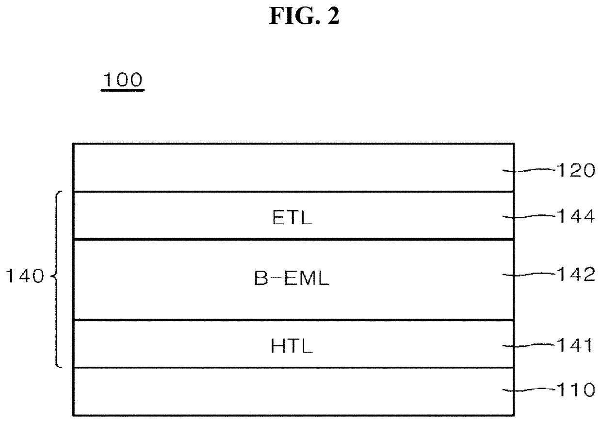
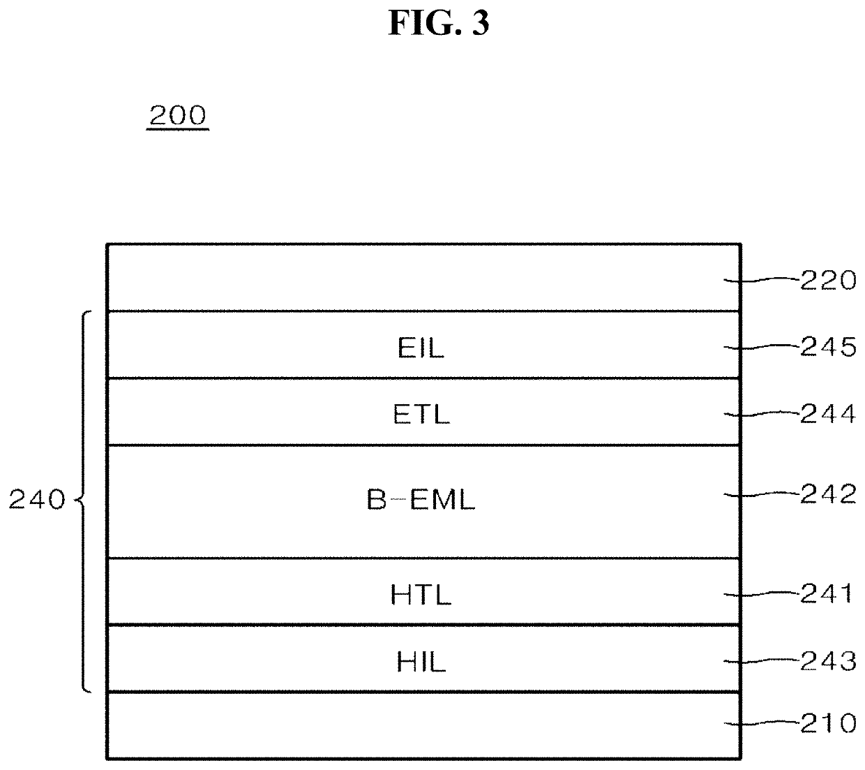
[0102]In a vacuum chamber at a pressure of 5×10⁻⁸ to 7×10⁻⁸ torr, an organic light-emitting diode was fabricated by sequentially depositing a hole injection layer, a hole transport layer (HTL1), a blue light-emitting layer (blue host material (BH) and blue fluorescent dopant material (BD, 4 wt % doping)), an electron transport layer (ETL1), an electron injection layer (LiF) and a cathode on an ITO substrate (anode).

[0103]FIG. 6 is an energy diagram depicting energy levels of an organic light-emitting diode of Example 1.

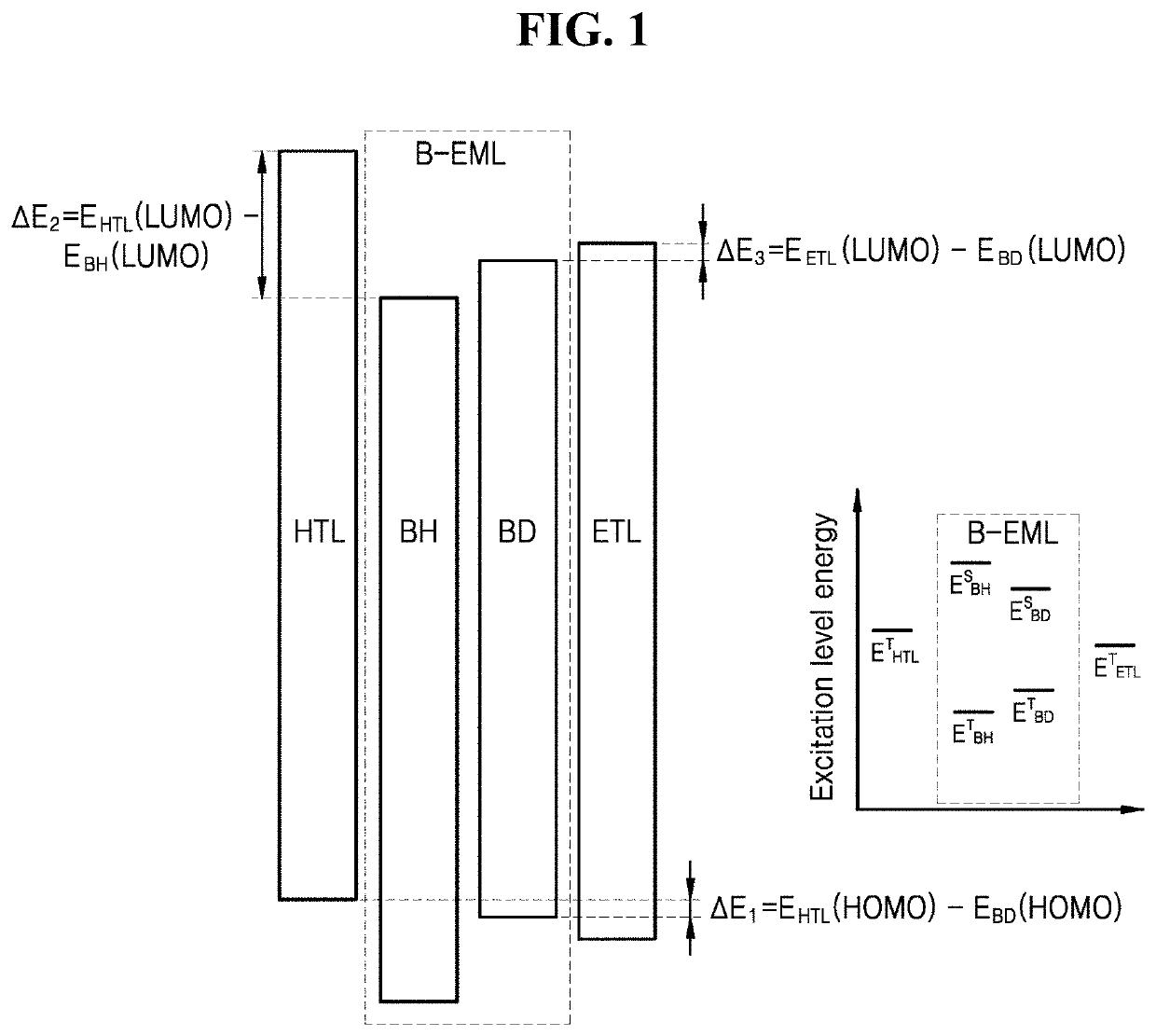
[0104]FIG. 6 is an energy diagram depicting the energy levels of HTL1 / BH+BD / ETL1 of the fabricated organic light-emitting diode. In evaluation of the energy level, it could be seen that, in the fabricated organic light-emitting diode, the difference between the HOMO energy level of HTL1 and the HOMO energy level of BD was 0.1 eV or less; the difference between the LUMO energy level of HTL1 and the LUMO energy level of BH was 0.5 eV or more; and the difference between ...

experimental example 1

ristics of Organic Light-Emitting Diode (Above)

[0110]Operation characteristics of the organic light-emitting diodes fabricated in Example 1 and Comparative Example 1 were evaluated. Table 1 shows voltage-current density, brightness-current efficiency, brightness-external quantum efficiency (EQE), and lifespan of the organic light-emitting diodes fabricated in Example 1 and Comparative Example 1.

[0111]

TABLE 1Voltage-currentBrightness-externalVoltagedensityquantum efficiencyLifespanItem(V)(Cd / A)(EQE)(hours)Example 13.78.08.150Comparative4.46.36.525Example 1

[0112]The organic light-emitting diode of Comparative Example 1 did not satisfy Conditions (E), (I), and (J). As a result, the organic light-emitting diode of Comparative Example 1 had a larger HOMO energy gap between HTL2 and BH than the organic light-emitting diode of Example 1 and low T1 energy (triplet energy). With reference to Table 1, in the organic light-emitting diode of Comparative Example 1, the HTL2 material had a triple...


PUM

PropertyMeasurementUnit
HOMO energy levelaaaaaaaaaa
LUMO energy levelaaaaaaaaaa

Abstract

An organic light-emitting diode includes: a first electrode, a light-emitting stack thereon including: a hole transport layer (HTL), a blue light-emitting layer including: a blue host material (BHM), and a blue fluorescent dopant (BFD) material, and an electron transport layer (ETL), and a second electrode on the light-emitting stack, wherein BFD LUMO>BHM, BFD HOMO>BHM, BFD singlet energy<BHM, HTL HOMO>BHM and BFD, HTL HOMO−BFD HOMO≤0.1 eV, the HTL material LUMO>the BHM, HTL LUMO−BHM LUMO≥0.5 eV, HTL LUMO>BFD, ETL LUMO>BHM and BFD, a difference in LUMO between the ETL material and the BFD material≤0.1 eV, and the HTL material, the ETL material, and the BHM have the following triplet energy relationships: T1,BH<T1,HTL and T1,BH<T1,ETL, 2.8<T1,HTL<3.0, and 2.6<T1,ETL<2.8.

Description

CROSS-REFERENCE TO RELATED APPLICATION(S)[0001]This application claims the benefit of and priority to Korean Patent Application No. 10-2017-0178316, filed on Dec. 22, 2017, the entirety of which is hereby incorporated by reference.BACKGROUND1. Technical Field[0002]The present disclosure relates to an organic light-emitting diode, an organic light-emitting display including the same, and a method of manufacturing the same.2. Discussion of the Related Art[0003]Recently, there is increasing interest in flat-panel display elements occupying a small space, with increasing size of displays. A technology of an organic light-emitting display including organic light-emitting diodes (OLEDs) as the flat-panel display elements has been rapidly developed in the art.[0004]An organic light-emitting diode emits light through conversion of energy of excitons created by pairs of electrons and holes generated upon injection of charges into an organic light-emitting layer formed between an anode and a ...

Claims


Application Information

Patent Timeline
Patent Type & Authority Patents(United States)
IPC IPC(8): H01L51/00H01L51/50H01L27/32H01L51/56H01L51/52H10K99/00
CPCH01L51/56H01L27/322H01L51/5072H01L51/5012H01L51/5278H01L51/5016H01L27/3244H01L51/5056H01L51/5004H01L51/0054H01L51/0072H01L51/005H01L51/0056H01L51/0058H01L2251/552H01L51/0074H10K85/622H10K50/11H10K2101/30H10K59/12H10K59/38H10K85/615H10K50/12H10K50/125H10K50/14H10K50/15H10K50/16H10K50/19H10K71/00H10K85/60H10K85/624H10K85/626H10K85/6572H10K85/6576H10K2101/40H10K2101/10
Inventor KIM, SANGBEOMSEO, JEONGDAE
Owner LG DISPLAY CO LTD
Learn More